My Latest Bad Idea#
Some people have hobbies, I find that cryptographic hashing accelerators are fascinating engineering challenges. Please hear me out.
Each algorithm offers slightly different design tradeoffs, presents unique opportunities for optimization, is easy to validate, and each serves as a perfect excuse to voluntarily subject yourself to a Friday evening of debugging hash result mismatches.
Now that the stage is set, let me introduce today’s star: BLAKE2. BLAKE2 is a family of cryptographic hash functions that takes arbitrary amounts of data and compresses it down to a variable-sized digest (hash). This hash is then used as a digital signature for message authentication codes and integrity protection mechanisms.
The BLAKE2 family comes in two primary variants:
- BLAKE2b, designed for 64-bit platforms
- BLAKE2s, the 32-bit variant
What makes BLAKE2 particularly interesting is that it was originally designed and optimized for high software performance. It’s fundamentally a software-first algorithm, in contrast to AES, which maps so clearly to hardware that your architecture practically writes itself as you read the spec.
This article will mostly focus on the why behind the design choices and not an in-depth presentation of the design itself. The full codebase can be found here :
For readers more interested in using this accelerator, the datasheet can be found here
Accessible, Not Easy#
The goal of this project was to independently tape out my first ASIC outside of any organized team.
This involves, solo: designing, validating, and successfully taping out a fully-featured BLAKE2s hashing accelerator on the SkyWater 130nm process through the Tiny Tapeout shuttle program.
A few years ago, independent ASIC tape-out would have been a pipe dream unless you had successfully sold your startup to Meta or grew up in a family whose garage included a private jet.
Today, thanks to recent advances in open-source EDA tools (Librelane, OpenROAD), the emergence of open-source PDKs thanks to Google (SkyWater 130nm, Global Foundries 180nm, IHP 130nm), and public low-cost shuttle programs like Tiny Tapeout that multiplex hundreds of designs onto shared chips, there now exists a path where independent designers can tape out custom ASICs without bankruptcy.
Some would say ASIC design has never been more accessible. This statement is technically true in the same way that saying running a marathon has never been as accessible : you can get a decent pair of running shoes from your local sports store, and running outside is free.
But accessible it is, and that’s revolutionary.
One Shot, Don’t Miss#
Unlike FPGA development and software where patches are possible, ASIC bugs are permanent, expensive, and occasionally end up as cautionary tales in textbooks.
As such, verification became my obsession. This verification strategy employed a multi-layered defensive line:
Simulation-based verification formed the foundation. The design results were simulated using cocotb against an instrumented golden model (hashlib’s blake2s version). Testing included both directed test cases for the official test vectors and constrained random stimulus generation for broader coverage. The goal wasn’t just functional correctness; it was finding the bugs that a directed-approach testing would miss.
FPGA emulation at the top, because hardware without software is just expensive modern art that occasionally gets warm.
Emulation provided the critical bridge between simulation and silicon. The design was ported to a Basys3 FPGA (Xilinx Artix-7, board chosen for its abundance of IO pins and next-day shipping on Amazon) and connected to an RP2040 microcontroller via GPIO, recreating the hardware/firmware interface planned for the final ASIC. This environment enabled co-design and validation of both the accelerator and its firmware, catching protocol issues and integration bugs that only manifest in the real hardware/MCU (MicroController Unit) setup.
Theory Meets Reality#
On the ASIC side, design correctness and timing passing were necessary but not sufficient.
An actual tape-out introduces the additional constraint of : can we actually build this? Can we get this to fit within the characterized operating parameters of the standard cells? AKA: if we do build it, will it work?
This challenge involves:
Design Rule Checking (DRC): for the SKY130A process, this meant staying within acceptable antenna ratios and keeping all the wire slew rates and max capacitances within PDK spec.
Shuttle-imposed limitations required designing within the constraints inherent to the Tiny Tapeout shuttle chip. The shared I/O architecture imposed severe bandwidth limitations: 66 MHz input maximum, 33 MHz output due to weak buffer drivers, and only 24 total pins for all communication.
These weren’t just inconveniences; they fundamentally shaped the architecture, capping performance more than any internal logic constraints.
What Comes Next#
This article goes through the process from idea to tape-out.
The chip is currently in fabrication, and in nine months, we’ll know if this produced a functional cryptographic accelerator or an expensive paperweight.
Open Source Silicon#
Before jumping deep into the weeds, I would first like to take a step back and give some context about the tools and shuttle program I will be using for this tape-out.
This won’t be an exhaustive list, and there are plenty of amazingly powerful tools that I won’t be mentioning. Think of it as a list of my favorites.
OpenROAD#
OpenROAD isn’t the name of a single tool as much as it is a family of ASIC design tools and is at the heart of the ASIC flow.
In conjunction with OpenSTA, which contains the timing engine, it includes the tools needed for taking a design from floorplanning through placement, clock tree synthesis, and routing all the way to finishing.
The official OpenROAD documentation has a great breakdown of some of the main features:
Here are the main steps for a physical design implementation using OpenROAD:
Floorplanning- Floorplan initialization - define the chip area, utilization
- IO pin placement (for designs without pads)
- Tap cell and well tie insertion
- PDN- power distribution network creation
Global Placement- Macro placement (RAMs, embedded macros)
- Standard cell placement
- Automatic placement optimization and repair for max slew, max capacitance, and max fanout violations and long wires
Detailed Placement- Legalize placement - align to grid, adhere to design rules
- Incremental timing analysis for early estimates
Clock Tree Synthesis- Insert buffers and resize for high fanout nets
Optimize setup/hold timingGlobal Routing- Antenna repair
- Create routing guides
Detailed Routing- Legalize routes, DRC-correct routing to meet timing, power constraints
Chip Finishing- Parasitic extraction using OpenRCX
- Final timing verification
- Final physical verification
- Dummy metal fill for manufacturability
- Use KLayout or Magic using generated GDS for DRC signoff
It was originally funded by DARPA, and this thought warms my aching heart when I see my tax bill.
LibreLane#
LibreLane is like a makefile that ties all of the ASIC tools together to build the ASIC flow. It pulls in Verilator for lint checking, Yosys and ABC for synthesis, OpenROAD for implementation, augmented with a few additional custom scripts to help complete the flow.
For this tape-out, we will be using the “classic” variant of the LibreLane flow.
Sky130A PDK#
The PDK, or Process Design Kit, is an integral part of making a digital ASIC design, as it contains the cell libraries and their characterizations for target operating parameters (temperature/voltage). It is literally the foundation upon which a digital design is built. Because of their nature, PDKs are foundry/process specific, each PDK is tailored by nature to a foundry/process and is typically designed by or in close cooperation with said foundry.
Typically, getting access to a PDK requires at least signing an NDA with a foundry and isn’t accessible to just anyone, so when Google partnered with the US-based SkyWater fab to release an open-source PDK for their 130nm process, it was very very significant. Google has additionally partnered with Global Foundries and released the gf180 for their 180nm MCU process. These open-source PDKs have truly changed what was possible for open-source silicon.
For this tape-out, I will be targeting a sky130A process. This is a classic CMOS process without the magnetic RAM that differentiates it from the sky130B process. More specifically, for this tape-out, I will be using the high-density cell library hd, which occupies a 0.46 x 2.72µm typical site, equivalent to 9 met1 tracks. As for the target typical operating parameters, it will be a temperature of 25C for a voltage of 3.3V.
Tiny Tapeout#
Tiny Tapeout is an open shuttle program where multiple projects are pulled together and taped out as part of the same chip. Participant projects are hardened as macro blocks, the size of which scales with the amount of purchased tiles. As such, projects range from the very tiny counter to the much larger SoC. These projects are multiplexed together behind a shared mux, connected to a shared bus, and use common I/O (with a few exceptions).
The final chip users can configure which project they want to enable during operation and all other designs will be power gated. The final chip is sold as part of a dev board, which contains both the Tiny Tapeout chip and is connected to an RP2040 MCU.
Architecture#
As I said in the introduction, something that I find makes hashing algorithms particularly interesting to implement is how the same functionality can be designed so differently given different PPA (power, performance, area) targets. And in this project, there were a few external constraints which, because of their importance, have defined the architectural direction.
BLAKE2 algorithme#
Before going deeper into our discussion of the architecture, in order to gain a better understanding of how our environment has shaped our architectural decisions, I would like to take a moment to delve in depth into the BLAKE2 algorithm to gain a better understanding of the problem itself.
As stated in the introduction, BLAKE2 is a hashing function. Its objective is to take a large amount of data and produce a high-entropy, reproducible shorter digest of this data, called a hash. This hash can then be compared against an expected hash result to identify if the data has been corrupted or tampered with.
Internally, the BLAKE2 hashing function breaks down the incoming data to be hashed into blocks (b) and passes each block through a compression function, during which the data will go through a few rounds of a mixing function. During this, a per-block internal state is computed (v), and the block result (h) is then derived from this internal state. The final hash result is derived from h and returned as the result on the last block.
The size of the data, as well as the number of mixing rounds, varies with the BLAKE2 variant:
- A block (b) is 64 bytes for BLAKE2s and 128 bytes for BLAKE2b
- The mixing function has 10 rounds for BLAKE2s and 12 rounds for BLAKE2b
- The mixing function internal state (v) size is 64 bytes for BLAKE2s and 128 bytes for BLAKE2b
- The block result (h) size is 32 bytes for BLAKE2s and 64 bytes for BLAKE2b
We can clearly see not only how BLAKE2b needs twice the storage requirement of BLAKE2s but also how large the memory footprint of BLAKE2, regardless of the variant is.
Pseudo code#
Pseudo-code for the blake2 function as per the rfc-7693 spec, we will make references to this latter in the article.
Mixing function G. R1, R2, R3, R4 and w are the constants given per blake2 version.
       FUNCTION G( v[0..15], a, b, c, d, x, y )
       |
       |   v[a] := (v[a] + v[b] + x) mod 2**w
       |   v[d] := (v[d] ^ v[a]) >>> R1
       |   v[c] := (v[c] + v[d])     mod 2**w
       |   v[b] := (v[b] ^ v[c]) >>> R2
       |   v[a] := (v[a] + v[b] + y) mod 2**w
       |   v[d] := (v[d] ^ v[a]) >>> R3
       |   v[c] := (v[c] + v[d])     mod 2**w
       |   v[b] := (v[b] ^ v[c]) >>> R4
       |
       |   RETURN v[0..15]
       |
       END FUNCTION.
Compression function F :
      FUNCTION F( h[0..7], m[0..15], t, f )
       |
       |      // Initialize local work vector v[0..15]
       |      v[0..7] := h[0..7]              // First half from state.
       |      v[8..15] := IV[0..7]            // Second half from IV.
       |
       |      v[12] := v[12] ^ (t mod 2**w)   // Low word of the offset.
       |      v[13] := v[13] ^ (t >> w)       // High word.
       |
       |      IF f = TRUE THEN                // last block flag?
       |      |   v[14] := v[14] ^ 0xFF..FF   // Invert all bits.
       |      END IF.
       |
       |      // Cryptographic mixing
       |      FOR i = 0 TO r - 1 DO           // Ten or twelve rounds.
       |      |
       |      |   // Message word selection permutation for this round.
       |      |   s[0..15] := SIGMA[i mod 10][0..15]
       |      |
       |      |   v := G( v, 0, 4,  8, 12, m[s[ 0]], m[s[ 1]] )
       |      |   v := G( v, 1, 5,  9, 13, m[s[ 2]], m[s[ 3]] )
       |      |   v := G( v, 2, 6, 10, 14, m[s[ 4]], m[s[ 5]] )
       |      |   v := G( v, 3, 7, 11, 15, m[s[ 6]], m[s[ 7]] )
       |      |
       |      |   v := G( v, 0, 5, 10, 15, m[s[ 8]], m[s[ 9]] )
       |      |   v := G( v, 1, 6, 11, 12, m[s[10]], m[s[11]] )
       |      |   v := G( v, 2, 7,  8, 13, m[s[12]], m[s[13]] )
       |      |   v := G( v, 3, 4,  9, 14, m[s[14]], m[s[15]] )
       |      |
       |      END FOR
       |
       |      FOR i = 0 TO 7 DO               // XOR the two halves.
       |      |   h[i] := h[i] ^ v[i] ^ v[i + 8]
       |      END FOR.
       |
       |      RETURN h[0..7]                  // New state.
       |
       END FUNCTION.
Main function :
       FUNCTION BLAKE2( d[0..dd-1], ll, kk, nn )
        |
        |     h[0..7] := IV[0..7]          // Initialization Vector.
        |
        |     // Parameter block p[0]
        |     h[0] := h[0] ^ 0x01010000 ^ (kk << 8) ^ nn
        |
        |     // Process padded key and data blocks
        |     IF dd > 1 THEN
        |     |       FOR i = 0 TO dd - 2 DO
        |     |       |       h := F( h, d[i], (i + 1) * bb, FALSE )
        |     |       END FOR.
        |     END IF.
        |
        |     // Final block.
        |     IF kk = 0 THEN
        |     |       h := F( h, d[dd - 1], ll, TRUE )
        |     ELSE
        |     |       h := F( h, d[dd - 1], ll + bb, TRUE )
        |     END IF.
        |
        |     RETURN first "nn" bytes from little-endian word array h[].
        |
        END FUNCTION.
Reality’s constraints#
Area#
A single sky130 Tiny Tapeout project tile is, as the name foreshadows, tiny… About 161x111.52 µm, or about as large as to realistically fit 256 bits worth of flip-flops on a good day.
Projects come in a set of varying sizes, from the smallest and more common single-tile project all the way to the 24-tile behemoth. But size isn’t the only thing that scales: cost scales too, with a single tile costing 70 euros. Projects thus range from 70 to 2240 euros.
So just like in the semiconductor industry, I have one of the best motivations to optimize for area: money.
Unfortunately, given the memory footprint intrinsic to the BLAKE2 algorithm, I had not chosen the most favorable project in the circumstance.
Storage#
At a minimum, I need to store:
- Current blocks: 64–128 Bytes (B)
- Internal state used by the mixing function: 64–128 Bytes (v)
- Current block result: 32–64 Bytes (h)
For context, a single tile can fit 440 bits, or 55 Bytes, of D-Flip-Flops at most, if you optimize solely for DFF count and push routing to the absolute limit. This is because D-Flip-Flop cells, a combination of two latches, are among the largest standard cells in the library.
To illustrate this area scale difference, here is the sky130_fd_sc_hd__and2_1 cell, a 2-input AND gate with a weak driver:
And here is the sky130_fd_sc_hd__dfxbp_1 cell, a standard complementary output D-Flip-Flop with the same weak output drive strength.
This flip-flop occupies five times the area of a simple AND gate. Yet, here we are looking to store, at the strict and very optimistic minimum, 3 to 6 tiles worth of flip-flops just to get this project off the ground.
But, when it comes to on-chip storage, I have two major issues:
There is currently no proven open-source SRAM for sky130. Although an experimental SRAM macro was submitted alongside this design on this shuttle, given that it is unproven, it would have risked losing the chip due to a bug.
D-Flipflop cells, now my primary source of storage, each take up a lot of area.
In a perfect universe, given the relatively massive amount of storage and the access pattern, storing data in SRAM would have been ideal. In practice, using flip-flops was my only feasible path. Given that the BLAKE2b variant requires twice the on-chip storage compared to the BLAKE2s version, this area constraint naturally guided the choice to implement the BLAKE2s variant.
I/O Bottleneck#
The objective was to tape out this design as part of the sky25b Tiny Tapeout shuttle. As such, this design will be integrated as a pre-hardened macro block into the larger chip. Like most blocks, it will communicate with the pins through a shared mux and will not own any pins on its own.

In addition to a reset and clock signal, each block is given access to the following I/O:
- 8 input pins
- 8 output pins
- 8 configurable input/output pins
Since these are the shuttle’s shared I/O, the design must respect whatever operating characteristics this shared I/O access imposes. This is where two additional limitations arise:
Firstly, the GPIO cell has a characterized maximum operating frequency of 66 MHz when operating above 2.2 V (we are operating at 3.3 V). In practice, this caps the maximum frequency at which we can operate the parallel bus between our MCU and our design over these pins.
Secondly, because of a weak driver on the output path (Design to MCU) leading to a slow slew rate, the maximum reliable operating frequency is capped at 33 MHz. This means that any transitions sent over the parallel bus must not exceed a transition frequency of 33 MHz, or signals risk being captured at the wrong level.
Putting it Together#
Given that additional metadata must be transmitted alongside the input data (and setting aside a few bits for handshaking with the MCU) we are left with only 8 bits in both the input and output directions for data transfer. Because each hashing round of the mixing function is performed on an entire block’s data, we must accumulate all 64 bytes of the next block before computation can begin.
This article is focused on explaining the rationale behind the design decisions rather than being a datasheet for the design itself.
So, just for context here is the final accelerator’s pinout:
| ui (Inputs) | uo (Outputs) | uio (Bidirectional) |
|---|---|---|
| ui[0] = data_i[0] | uo[0] = hash_o[0] | uio[0] = valid_i[0] |
| ui[1] = data_i[1] | uo[1] = hash_o[1] | uio[1] = cmd_i[0] |
| ui[2] = data_i[2] | uo[2] = hash_o[2] | uio[2] = cmd_i[1] |
| ui[3] = data_i[3] | uo[3] = hash_o[3] | uio[3] = ready_o |
| ui[4] = data_i[4] | uo[4] = hash_o[4] | uio[4] = output_mode_i[0] |
| ui[5] = data_i[5] | uo[5] = hash_o[5] | uio[5] = output_mode_i[1] |
| ui[6] = data_i[6] | uo[6] = hash_o[6] | uio[6] = |
| ui[7] = data_i[7] | uo[7] = hash_o[7] | uio[7] = hash_valid_o[7] |
Additionally, due to area limitations, we cannot afford the extra 64 bytes of memory required to pipeline this accumulation in parallel with the previous block’s computation. As such, the computation is stalled while the next block’s data is being received.
To comply with the GPIO operating frequency limit, we could have operated the accelerator at 33 MHz to align the input bus frequency with the output frequency. However, because of the bottleneck imposed by the significant number of cycles required to transfer the next block of data, maintaining the highest possible input bus frequency was paramount. Consequently, I decided to operate both the input and output buses at 66 MHz and compensate for the slow slew rate by holding data on the output interface for two clock cycles.
While it would have been technically possible to introduce a faster internal clock domain to the accelerator and add a clock domain crossing (CDC) between the internal logic and the I/O interfaces, it would have yielded little improvement. Since a faster internal clock would only accelerate the computation phase, and the design is primarily bottlenecked by the time spent waiting for input block data, the overall performance gain would be negligible.
Design#
Given these external constraints, the design direction was clear: a BLAKE2s implementation using on-chip D-FlipFlops for storage, focusing on area optimization and a target operating frequency of 66 MHz.
The design described by the following section can be found on my github repository
Hash Configuration#
During each hash function run, the internal state (h) is calculated based on a set of per-run configuration parameters, either during the initialization of the first block or during the initialization of the last block. These values are:
kk: Key length in bytesnn: Resulting hash length in bytesll: Total length of the data to be hashed
In the software implementation, these are passed to the BLAKE2s function as arguments. In our design, since we cannot derive these from the input data, we need a way to acquire these configuration parameters before the hash computation begins.
As such, a configuration parameter transfer packet exists in parallel to the block data transfer packet. This packet is sent over the same 8-bit data input interface and is differentiated from data transfers by the state of the data mode pins.
The packet follows a little-endian layout, when sending multi-byte arrays, the lower indices are sent first:

The byte_size_config module (located under the io_intf module) identifies these configuration packets, parses and latches them. It outputs the most recent values of kk, nn, and ll directly to the main hashing modules. Consequently, the same configuration can be reused across multiple runs of the accelerator.
link to code: byte_size_config
Block Data Buffering#
A block of data needs to be streamed over 64 cycles from the MCU to the ASIC. Like with the config parameter, there is a module dedicated in the design to tracking this data arrival, but because of the size of the buffer, directly translating to the area occupied by dffs, needed to hold this data, the block isn’t stored in memory in this module (and its content aren’t held stable over an interface destined for the main hashing module). Rather, this module contains only the logic needed to identify when data is being received, the data offset, and a flopped copy of the most recent byte. On the main hashing module side, these signals are received and used to determine the appending of the next incoming data byte to the block buffer.
This split allows there to be only the strictly necessary logic dedicated for the block data reception in the main hashing module (blake2s), while putting the majority of the block data streaming logic in the block_data module, also under io_intf.
Now, earlier I said that a byte index was included in the signals sent from the block_data to the main hashing module blake2s.
Contrary to what intuition might suggest, this byte index isn’t used to address the buffer on writes. The reason why is that this would require a 1-to-64 x8-wide demux logic to implement, which would be quite expensive in terms of area. Rather, we are using a less expensive shift buffer for writes, which also happens to perfectly fit this application given that bytes are streamed in order to the ASIC.
Toivoh did a great study that can be found here: https://github.com/toivoh/tt08-on-chip-memory-testThis byte index is actually used to keep track of the completion of the block data so that the main hash module can start computing the hash as soon as the full block has been received. block_data
Mixing Function#
The mixing function is at the heart of the hashing function and is also the critical path in the main loop of the hashing logic. It is called 8 times per round using different data as input, for 10 rounds.
       |      |   // Message word selection permutation for this round.
       |      |   s[0..15] := SIGMA[i mod 10][0..15]
       |      |
       |      |   v := G( v, 0, 4,  8, 12, m[s[ 0]], m[s[ 1]] ) // 0
       |      |   v := G( v, 1, 5,  9, 13, m[s[ 2]], m[s[ 3]] ) // 1
       |      |   v := G( v, 2, 6, 10, 14, m[s[ 4]], m[s[ 5]] ) // 2
       |      |   v := G( v, 3, 7, 11, 15, m[s[ 6]], m[s[ 7]] ) // 3
       |      |
       |      |   v := G( v, 0, 5, 10, 15, m[s[ 8]], m[s[ 9]] ) // 4
       |      |   v := G( v, 1, 6, 11, 12, m[s[10]], m[s[11]] ) // 5
       |      |   v := G( v, 2, 7,  8, 13, m[s[12]], m[s[13]] ) // 6
       |      |   v := G( v, 3, 4,  9, 14, m[s[14]], m[s[15]] ) // 7
FUNCTION G( v[0..15], a, b, c, d, x, y )
|
| v[a] := (v[a] + v[b] + x) mod 2**w
| v[d] := (v[d] ^ v[a]) >>> R1
| v[c] := (v[c] + v[d]) mod 2**w
| v[b] := (v[b] ^ v[c]) >>> R2
| v[a] := (v[a] + v[b] + y) mod 2**w
| v[d] := (v[d] ^ v[a]) >>> R3
| v[c] := (v[c] + v[d]) mod 2**w
| v[b] := (v[b] ^ v[c]) >>> R4
|
| RETURN v[0..15]
|
END FUNCTION.In an ideal world, from a performance perspective, I could have parallelized all of these 8 iterations in a single cycle. But this is reality and there are 3 limitations with this approach:
The design direction of this ASIC is to optimize for area, and the additional logic incurred by this technical decision would be very expensive in terms of area.
There are data dependencies between v array values due to reused indexes.
The full path through a single G function, including the data reads, was 69 logic levels deep at its maximum and is much too long to fit in a single 66MHz cycle. So at a minimum, we are looking at 2 cycles.
Because of the above, this approach isn’t technically feasible, and even if it was, the area expense might not have been worthwhile, as extra area could be better expensed elsewhere, for example, for adding a second block buffer to allow streaming the next block in parallel with hashing a current block.
The initial approach was to split the critical path through the G function into 2 cycles. This resulted in a 100% reduction of the hashing function performance, but this represents only a drop of 55% of the overall system performance when taking into account the block streaming dedicated cycles.
link to code: G function main code
This helps solve part of our timing issue, but the path is still quite deep due to the data read section at the start of this path.
As readers can imagine, the data read paths are bloated by a number of large muxes for obtaining v[a], v[b], v[c], v[d], x, and y. There isn’t much optimization to be done for x and y, obtained from m[s[<current index>]] given s varies per round and spans all indexes of m. But there is some optimization we can squeeze out for the v vector accesses.
Looking closer at the code, a, b, c, and d can each take a set of only 4 possible values, depending on the current G function call. By reworking the logic we can force the instantiation of only a 4-way muxing logic, greatly reducing logic cost and depth at the cost of some slightly more complex RTL.
Now we have reduced the logic on our read path, timing is looking good, but the G function still takes 2 cycles, and although we are not optimizing primarily for performance, leaving so much performance on the table is … unfortunate. Luckily, looking closer at the algorithm, we can spot a few additional critical nuances:
The m vector is not modified during a round, only read, so we can be flexible with the ordering of its reads.
The a, b, c, and d indexes used to read and write the v vector when calling Gn not overlap with Gn+1
for n ∈ {0,1,2,4,5,6}. Though, there is overlap for n=3, d=15 and n=7,b=4.
With these observations, we can start pipelining our G function path. By this I mean, we can start the next G function instance as the previous instance is still going through its second cycle. Though because of the data dependencies noted for instances n=3 and n=7, this pipelining isn’t perfect, and a nop cycle is imposed in order for the new values of v[d] and v[b] to become available for the next data read.
With this optimization, we can drastically drop the penalty on the hashing from 100% to 25%, with the overall performance penalty dropping from 55% to only 11%.
Output Streaming#
At the very end of the hash computation, the ASIC starts streaming out the hash result. Even though 32 final hash bytes have been computed, only the first nn bytes will be streamed out (dependent on the nn configuration parameter). Due to our slow slew rate on the output GPIO buffer (the electrical equivalent of low blood pressure), a “slow output mode” was designed to hold each data transfer out of the ASIC over 2 cycles rather than one, leaving enough time for the signal to settle on the output pins.
The output streaming logic lives in the main hash module blake2s, but result streaming doesn’t block the FSM from starting to wait for the next start of the block to stream in.
link to code: output streaming
Co-designing Firmware#
When it comes to designing a master for this hashing accelerator ASIC, my two main options were an FPGA or an MCU. Designing for an FPGA would have been simpler, given that an FPGA’s flexibility, configurability, and timing accuracy make it well-adapted for high-speed custom protocols. The downside to this approach was that it would require users other than myself to have a similar FPGA setup if they wished to interact with my design.
As such, even at the cost of more effort, my objective was to have this design interface with the MCU shipped on the Tiny Tapeout dev board. Fortunately, the chosen chip was none other than the Raspberry Silicon RP2040.
The new lineup of MCU silicon developed by Raspberry includes an unusual hardware block called the PIO (Programmable Input/Output), which is a tiny co-processor that allows for pin reads and writes in a deterministic and cycle-accurate fashion. Without going too far off-topic into the details, this is perfect for designing custom high-speed parallel bus protocols and supports my upper target of 66 MHz.
The problem is that the PIO co-processor is tiny and supports only a subset of operations. As such, this custom bus protocol must be designed around the MCU hardware’s capabilities.
Bubbles in Data Transfer#
As established earlier, the block data is transferred from the MCU to the ASIC 8 bits at a time. Each block is 64 bytes long, so ideally, this transfer would be completed over 64 consecutive cycles. In practice, however, even though continuous transfer is the norm, a corner case exists where the MCU can introduce random gaps in the middle of block streaming.
To understand why these empty cycles occur, we need to take a step back and understand how data accesses work in the PIO. Each PIO is divided into four State Machines (SM) that can each independently run a pio program. Our block streaming program runs on one such SM.
Internally, each SM is equipped with very little storage, as memory being expensive in terms of area is a universal struggle. Each SM can be configured to have up to 8x32 bits of FIFO storage, with up to 32 aligned bits accessible each cycle and a 32-bit wide output buffer. To write to a pin, we must first pull a full 32-bit FIFO entry into the output buffer, and only then can we write the contents of the output buffer to the pins. The PIO hardware allows us to configure the FIFO so that when the output buffer has been read to a trigger point, it automatically pulls the next available entry from the FIFO. Issues arise when the FIFO becomes empty and needs to be refilled.
This SM program writes to the parallel bus operating at 66 MHz. The RP2040 features a dual-core Cortex-M0+, and programs running on it are, to put it delicately, “slower than hardware.” I cannot rely on a software program to poll the FIFO state and refill it as soon as an entry is free, as software runs orders of magnitude too slowly.
Luckily, the RP2040 has a DMA (Direct Memory Access) system to which I can offload this exact task : given an array in memory, it starts a 32-bit wide transfer from the next unread section of memory to the SM FIFO. This DMA is designed to be able to keep up with the PIO SM speed. However, in very rare corner cases, since the DMA is a shared component using shared internal buses, it might be stalled for a few cycles, resulting in bubbles being introduced during block streaming.
Because of this, both the parallel bus protocol and the ASIC must accommodate empty cycles during data streaming for both block data and for the same reason, the configuration parameter packets.
Handshaking for Block Streaming#
This ASIC can hash multiple blocks consecutively. However, since the internal block storage is reused for both streaming data in and performing the hashing operation, the design does not support streaming a new block while hashing is in progress. Having the MCU keep track of when the ASIC is ready to receive the next block would be too imprecise and would leave too much performance on the table, as we would have to overshoot the timing estimate to avoid data corruption.
To solve this, the parallel bus protocol includes a data_ready_o signal that indicates to the MCU that the hardware is ready to accept a new block. As soon as the SM (State Machine) detects this signal, it knows it is safe to start streaming the next block.
With this implementation, the SM data write program sequence becomes :
- Wait for
data_ready_oto be asserted. - Wait for data to be available in the FIFO.
- Synchronize with the clock.
- Stream out data until the block transfer is complete.
- Repeat.
link to code: data write pio program
Result Valid#
The PIO co-processor instruction set is small and simple, featuring only nine different instructions. Notably, there is no single “read on signal asserted” instruction. The “wait for signal” and the “read from pin” instructions are separate, and since each instruction takes one cycle to execute, we cannot assert the result valid signal at the exact moment we start the data transfer. We must do so at least one cycle beforehand.
As such, our parallel protocol requires the ASIC to assert the hash_valid_o signal one cycle before data starts flowing. This gives the state machine program enough time to identify the event and transition to the data capture routine. In a way, this is the digital equivalent of yelling “INCOMING!” before throwing your precious hash results overboard.
link to code: hash read pio program
Result to Memory#
The hash results are of variable length, with a maximum length of 32 bytes. Receiving and reading the incoming hash result from the ASIC to the MCU memory is handled by a separate PIO SM (State Machine). This SM has its own 8×32 bits deep RX FIFO in which incoming data can be buffered. However, this RX FIFO is, yet again, too small to capture the full hash on its own, even if we only read 8 bits (from 8 pins) per cycle as we do on the emulator.
ui_in[0-3] placed in the middle of the uo_out pins, we face a mapping challenge. Since the PIO hardware can only read and write consecutive pins, and we want our data to be aligned on 32-bit boundaries, the final version will require reading 16 bits each cycle to capture the necessary 8 bits.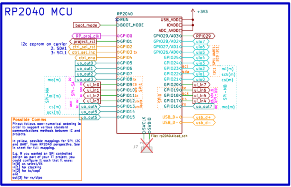
Here again, the Cortex-M0+ cores are too slow for our use case, so we rely on the DMA to copy the contents of the full FIFO entries to memory. Unlike the data streaming example, where we could tolerate gaps, here we must guarantee that no bubbles are introduced in the read sequence. In this context, bubbles would occur if the RX FIFO and the input buffer were full, causing the pin read to stall until space became available, and dropping all incoming bytes in the meantime.
The RX FIFO could reach capacity if our RX to memory DMA transfer were stalled by another peripheral using the shared internal hardware resources, such as a concurrent block data DMA transfer to a different state machine on the same PIO.
To prevent this scenario, we configure the DMA engine to give the highest priority to our transfer.
link to code: set DMA high priority
Implementation#
As this article is already getting quite long (congratulations for sticking around), I won’t delve too deeply into the implementation issues encountered while iterating on this design. I will simply say that implementation runs were performed regularly in parallel with the design work to quickly identify and refine timing while keeping area utilization in check.
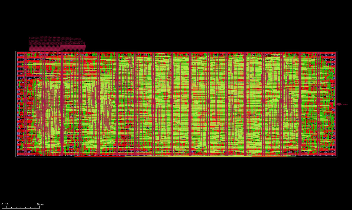
When it comes to violations, antenna issues were the primary challenge because this ASIC targets Sky130A and the chosen layout was a very long 4×2 tile rectangle. Some of these wires were so long they practically had multiple postal codes. This is also why, when looking at the cell frequency table, readers can see the scars of battle in the form of the design being covered in diodes. These were used to offer discharge paths for charges accumulated during fabrication:
| Cell type | Count | Area |
|---|---|---|
| Fill cell | 6073 | 30445.45 |
| Tap cell | 2158 | 2700.09 |
| Diode cell | 4031 | 10087.17 |
| Buffer | 66 | 251.49 |
| Clock buffer | 91 | 1238.69 |
| Timing Repair Buffer | 1892 | 16809.87 |
| Inverter | 89 | 380.36 |
| Clock inverter | 28 | 341.58 |
| Sequential cell | 1657 | 33324.46 |
| Multi-Input combinational cell | 5638 | 53603.91 |
| Total | 21723 | 149183.08 |
The heuristic addition of diodes by the tools helped fix many of the major issues, but there were still a few remaining. Since antenna violations only translate to a probabilistic increase in defect rates, leaving a few minor violations should be unnoticeable. However, for the few major violations remaining, I manually added buffer cells to these paths to break them apart:
    // manually inserting buffers for fixing implementation
    genvar buf_idx;
    generate
        for(buf_idx = 0; buf_idx < W; buf_idx=buf_idx+1) begin: g_buffer
            `ifdef SCL_sky130_fd_sc_hd
            /* verilator lint_off PINMISSING */
            sky130_fd_sc_hd__buf_2 m_c_buf( .A(g_c_buf[buf_idx]), .X(g_c[buf_idx]));
            sky130_fd_sc_hd__buf_2 m_y_buf( .A(g_y_buf[buf_idx]), .X(g_y[buf_idx]));
            /* verilator lint_on PINMISSING */
            `else
            assign g_c[buf_idx] = g_c_buf[buf_idx];
            assign g_y[buf_idx] = g_y_buf[buf_idx];
            `endif
        end
    endgenerate
A few minor violations remained (P/R: 2.65, 1.26, and 1.02); these should be acceptable and are unlikely to cause any noticeable yield degradation, so I decided to let them through. Apart from these antenna violations, there are no other known issues in this implementation.
The ASIC has now been taped out and is in fabrication as part of the Tiny Tapeout sky25b shuttle , with an estimated delivery date of June 30, 2026.
Conclusion#
This project has been a game changer for me.
My previous RTL engineering experiences in CPU at ARM and on FPGAs at Optiver were mostly focused on design and verification, and only gave me a restricted picture of what end-to-end chip tapeout really is.
We live in an interesting history period, where it is realistic for someone to fully design and tape out their own ASIC, as long as they have enough learning motivation and sanity to spare. It is rather unprecedented, and I am not sure if it will last, as the actual business model of such manufacturing processes is still to be established.
But in the meantime, it represents a gigantic learning opportunity for designers, and I can’t stress that enough. For someone like me who hugely values technical skills, opensource PDKs are a gold mine. In a couple of months, armed with patience, a couple of all nighters, and a megaton of coffee, homemade tapeout went from an unrealistic dream to an actual reality.
Even if the accelerator itself was “relatively” simple (a sort of blinky project on steroids, one might say), the real difficulty was in correctly understanding the entire ASIC design flow, the many tools and steps involved, and the new constraints imposed by the fact that at the end, it had to run on actual silicon, and work on first try.
It did cost a lot of time and energy but it was definitely worth the shot and I would recommend the interested designer to have a try at it, given how much they will learn from it.