Introduction#
When doing embedded systems development, it can sometimes be hard to find a development board with the desired features at an affordable price. A solution to this is to learn how to design and manufacture your own custom development boards.
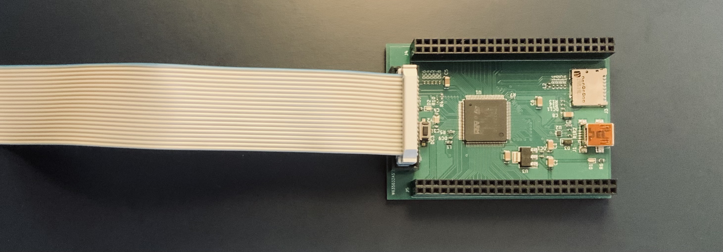
This project is my first custom development board. It features :
- the
STM32H750VBT6TRMCU containing anARM cortex-m7core; - an
SWDdebug interface with a pinout compatible with the 20 pin J-Link probe; - an
USB-B miniconnector; - a
Micro SDcard connector.
An anniversary present#
I met my wonderful husband over 10 years ago, we were high school love birds.
Today he is a talented low level C developer that writes kernels for fun.
He likes targeting microcontrollers but was often disappointed by the lack of proper JTAG
or SWD debugging interface on all the development boards he owned.
As such, this board was made as my 10 year anniversary present to him.
Debug interface#
One of the goals on this design is to be able to directly plug the debug probe onto the board without the need for any additional adapter.
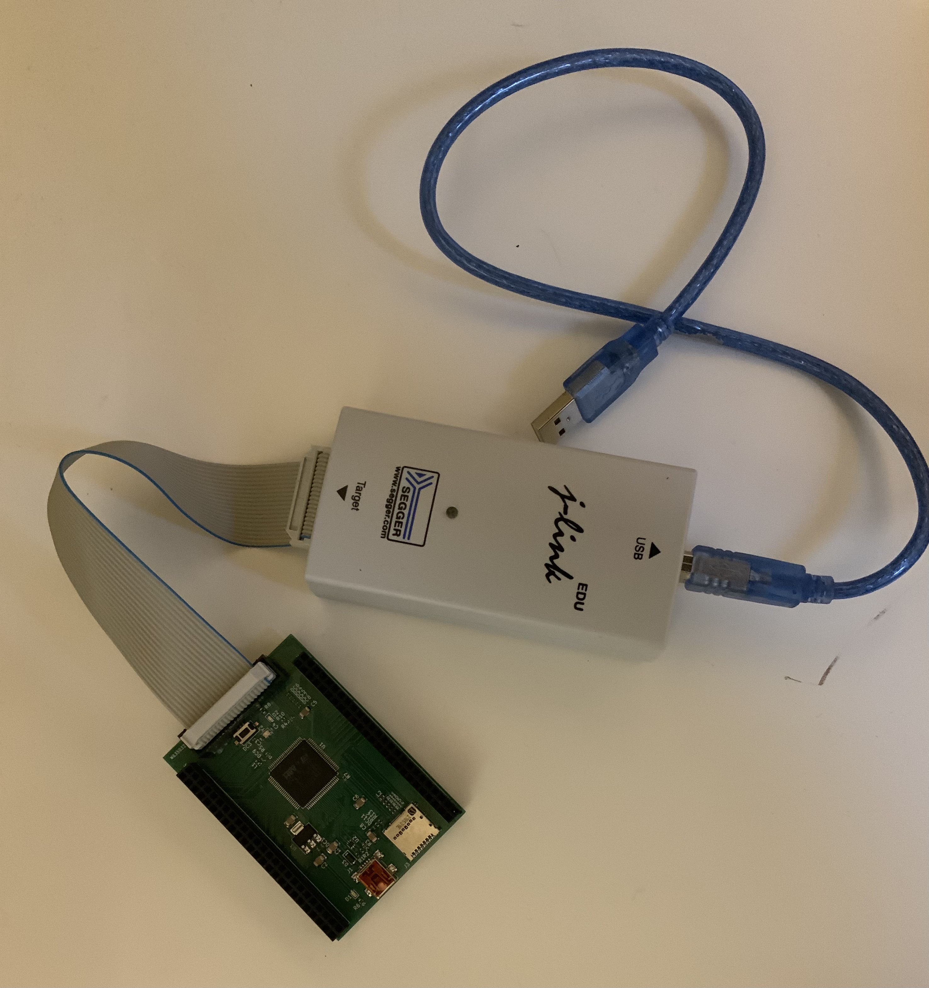
J-Link connector pinout#
We are using a J-Link as our debug probe. It has a 20 pin connector and supports SWD using the following connector pinout:

The following table lists the J-Link / J-Trace SWD pinout.
| Pin | Signal | Type | Description |
|---|---|---|---|
| 1 | VTref | Input | This is the target reference voltage. It is used to check if the target has power, to create the logic-level reference for the input comparators and to control the output logic levels to the target. It is normally fed from Vdd of the target board and must not have series resistors. |
| 2 | Vsupply | NC | This pin is not connected in the J-Link. It is reserved for compatibility with other equipment. Connect to Vdd or leave it open in target system. |
| 3 | Not used | NC | This pin is not used by the J-Link. If the device may also be accessed via JTAG, this pin may be connected to nTRST, otherwise leave it open. |
| 5 | Not used | NC | This pin is not used by the J-Link. If the device may also be accessed via JTAG, this pin may be connected to TDI, otherwise leave it open. |
| 7 | SWDIO | I/O | Single bi-directional data pin. |
| 9 | SWCLK | Output | Clock signal to target CPU. It is recommended that this pin is pulled to a defined state of the target board. Typically connected to TCK of target CPU. |
| 11 | Not used | NC | This pin is not used by the J-Link. This pin is not used by J-Link when operating in SWD mode. If the device may also be accessed via JTAG, this pin may be connected to RTCK, otherwise leave it open. |
| 13 | SWO | Input | Serial Wire Output trace port. (Optional, not required for SWD communication.) |
| 15 | nRESET | I/O | Target CPU reset signal. Typically connected to the RESET pin of the target CPU, which is typically called “nRST”, “nRESET” or “RESET”. This signal is an active low signal. |
| 17 | Not used | NC | This pin is not connected in the J-Link. |
| 19 | 5V-Supply | Output | This pin is used to supply power to some eval boards. |
Pins 4, 6, 8, 10, 12, 14, 16, 18, 20 are GND pins connected to GND in J-Link. They should also be connected to GND on the board.

All SWD J-Link pins are connected with the exception of the 5V-Supply,
as even when the debug probe is connected power is still gotten from the USB.
Mounting the connector to the PCB#
The connector should be mounted with the slot facing up, away from the MCU as shown below.

CAD#
This board was designed using Kicad 7.0.8 and all project files are
available for download in the following github repository.
Schematic#
Full schematics of the board :

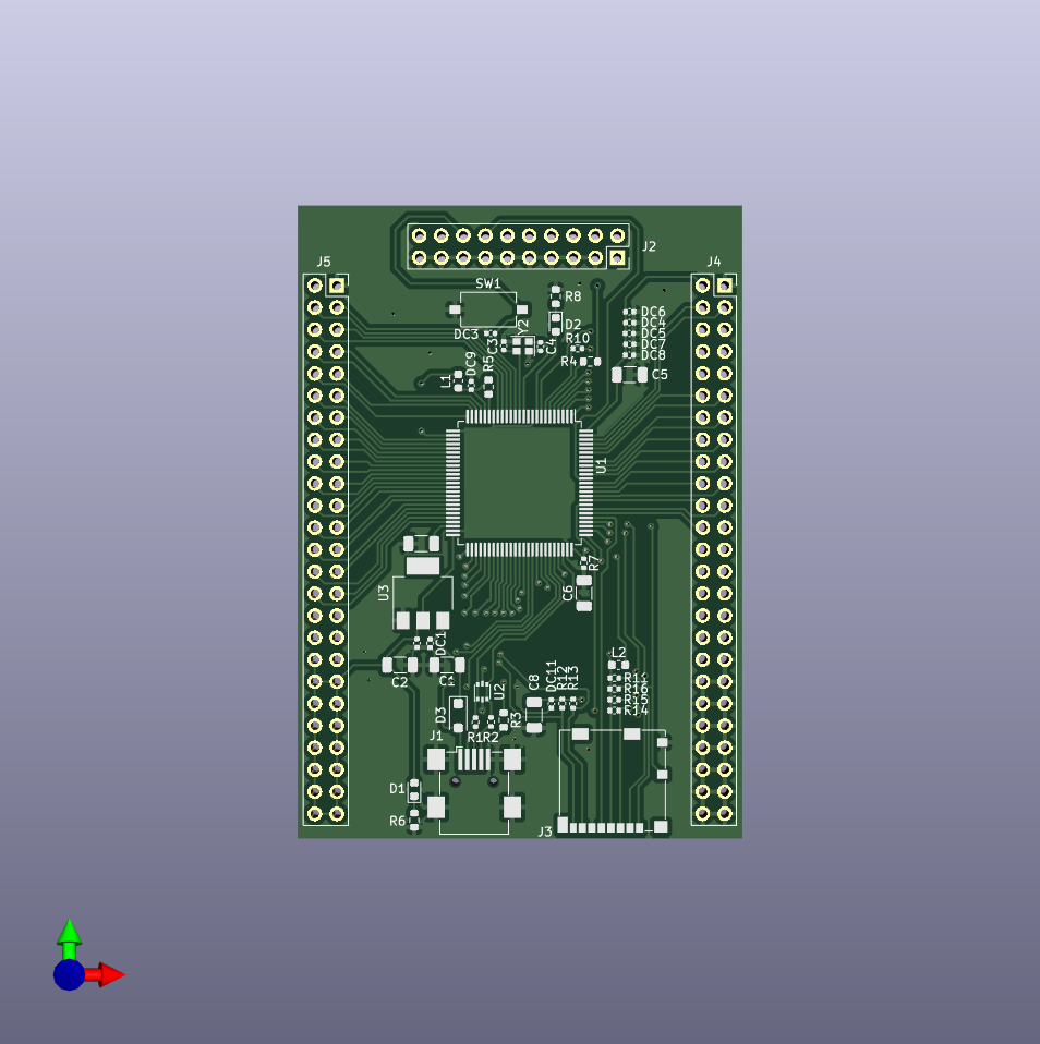
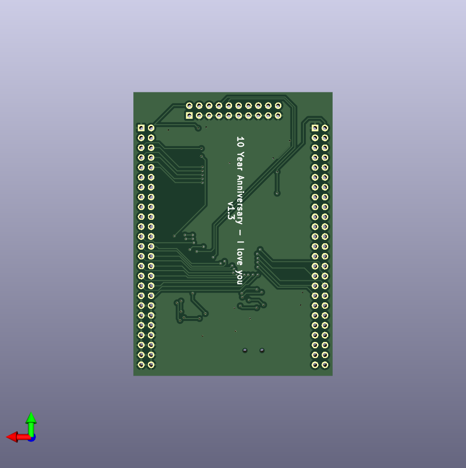
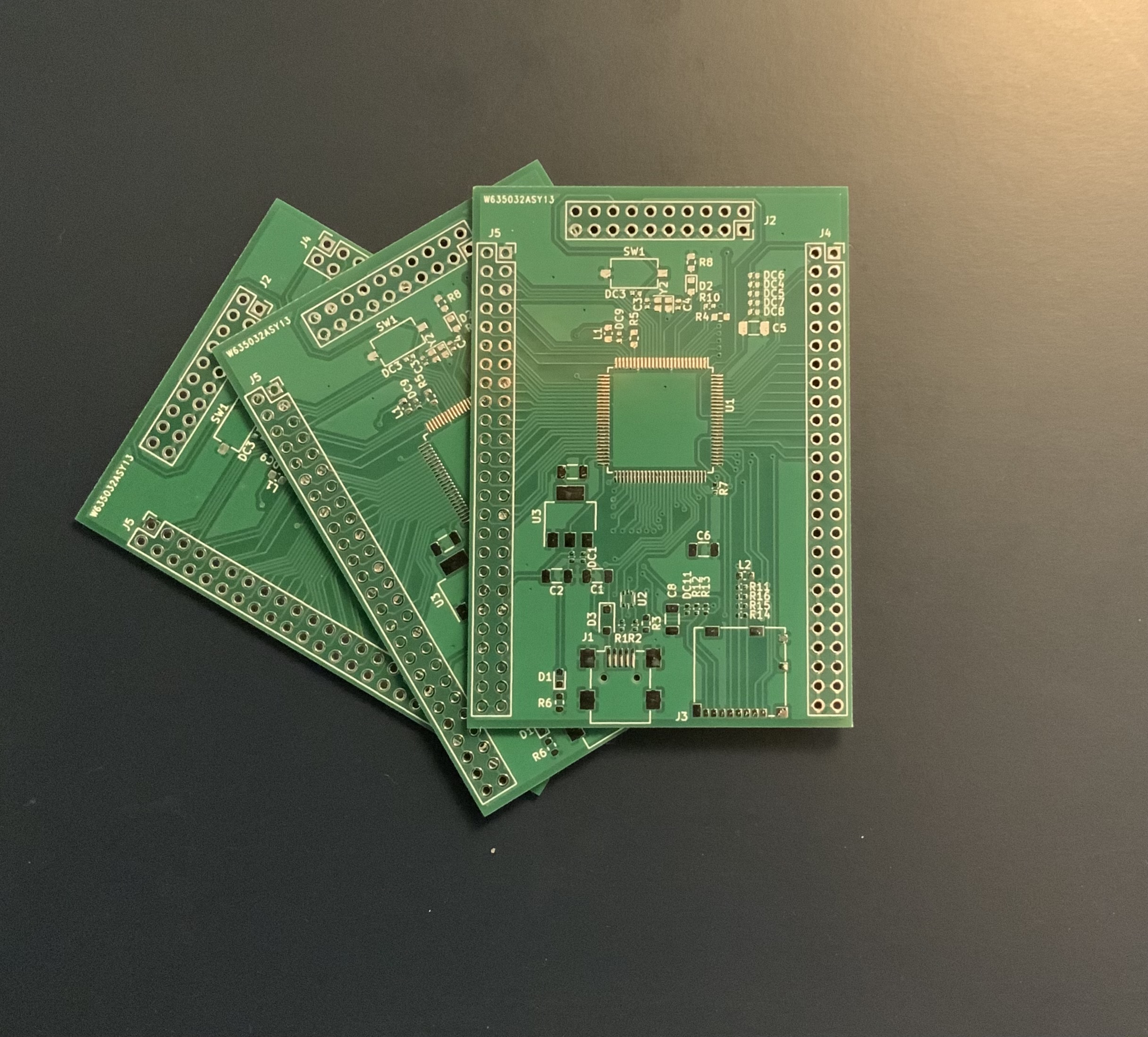
PCB#
Computer rending of the PCB :
Final result :
Bill of Materials#
| Item # | Designator | Qty | Manufacturer | Mfg Part # | Description / Value | Package/Footprint | Type | Your Instructions / Notes |
|---|---|---|---|---|---|---|---|---|
| 1 | DC6,DC3,DC5,DC4,DC8,DC9,DC7,DC11,DC1,DC2 | 10 | KEMET | C0402C104K4RAC | 100nF | 0402 | SMD | |
| 2 | U3 | 1 | Texas Instruments | TLV1117-33CDCYRG3 | TLV1117-33 | SOT-223 | SMD | |
| 3 | R4,R5,R3 | 3 | SEI Stackpole | RMCF0603JJ1K00 | 1k | 0603 | SMD | |
| 4 | Y2 | 1 | ECS Inc. | ECS-250-9-37B2-CKM-TR | 25MHz 9uF | 2.0x1.6mm | SMD | |
| 5 | R15,R14,R13,R7,R16,R12,R10,R11 | 8 | YAGEO | RC0402FR-0710KL | 10k | 0402 | SMD | |
| 6 | U1 | 1 | STMicroelectronics | STM32H750VBT6TR / STM32H742VIT6 | STM32H750VBTx / STM32H742VI | LQFP-100 | QFP | MCU for v1 and v2, pin compatible |
| 7 | J2 | 1 | On Shore Technology Inc. | 302-S201 | Conn_ARM_JTAG_SWD_20 | THD | Through Hole | |
| 8 | C8,C5,C6,C7,C1,C2 | 6 | Samsung Electro-Mechanics | CL31A476MQHNNNE | 47uF/3528 | 1206 | SMD | |
| 9 | D2,D1 | 2 | EVERLIGHT | 19-213SYGC/S530-E2/5T | LED | 0603 | SMD | |
| 10 | R1,R2 | 2 | YAGEO | RC0402FR-0722RL | 22 | 0402 | SMD | |
| 11 | R6,R8 | 2 | SEI Stackpole | RMCA0603JT510R | 510 | 0603 | SMD | |
| 12 | C4,C3 | 2 | Murata Electronics | GJM1555C1H8R0DB01D | 8pF | 0402 | SMD | |
| 13 | J3 | 1 | Molex | 1040310811 | Micro_SD_Card_Det1 | SMD | ||
| 14 | D3 | 1 | Toshiba | CRS30I40A(TE85L,QM | SS34 | SOD-123F | SMD | |
| 15 | L1,L2 | 2 | TAI-TECH | FCM1608KF-102T02 | 1KB | 0603 | SMD | |
| 16 | SW1 | 1 | C&K | PTS636 SM43 SMTR LFS | SW_RESET | 6.0x3.5mm | SMD | |
| 17 | U2 | 1 | STMicroelectronics | USBLC6-2P6 | USBLC6-2P6 | SOT-666 | SMD | |
| 18 | J1 | 1 | Adam Tech | MUSB-B5-S-RA-SMT-PP-T/R | USB_B_Mini | SMD | ||
| 19 | J4,J5 | 2 | Sullins Connector Solutions | PPTC252LFBN-RC | Conn_02x25_Odd_Even | Through Hole |
For reference, I recently ordered components for 3 version 2 boards in Canada and spent 107 CAD
at Mouser.
Version 2#
Now that the first version is up and running it is time to start thinking of improvements for the second version.
The first revision of the board uses the STM32H750VBT6TR MCU, which only has 128kB of flash.
Now that I have confirmed that the board is working it is time to
upgrade to something with more flash.
This new revision will keep the existing PCB and components but
drop in the STM32H742VIT6 as the MCU.
This MCU features 2 MB of flash, 1 MB of RAM and is otherwise the same chip with regards to the features that matter to us.