Well that was a ride, where do I start ?
I am currently on a quest to build some open source networking equipment with the final boss being a full router.
There are a lot of very valuable and less complex pieces of hardware on the way that also need building, one of them being the common networking switch.
Previously I was building the infrastructure to handle ethernet packets and worked my way up to a simple three-port switch that I had taped it out via Tiny Tapeout. But a few days after that tapeout, as I was still reeling from the adrenaline of rushing to meet the deadline, an unexpected opportunity presented itself: the possibility of taping out my own full chip, free of charge!
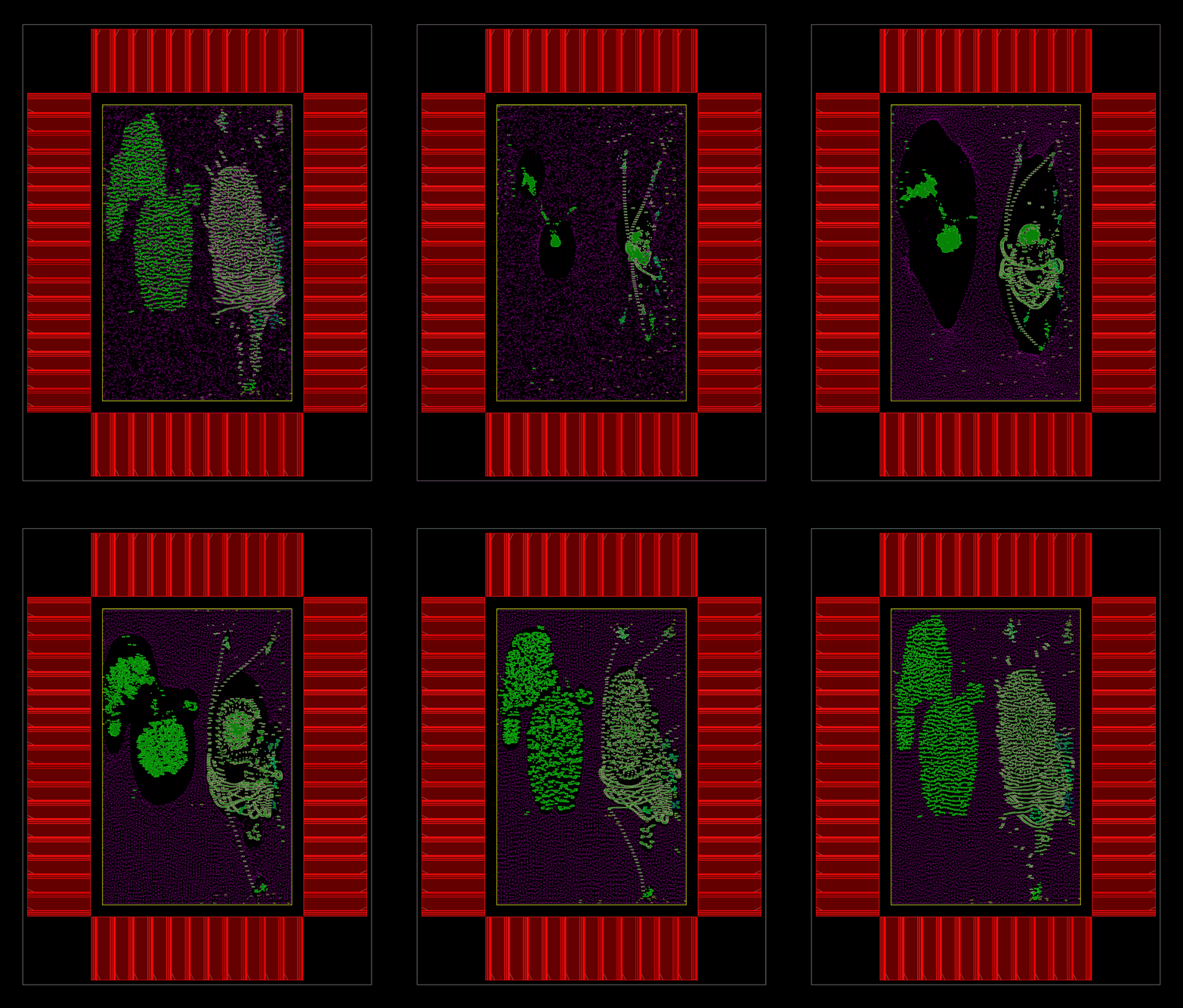
But there was one slight problem, I only had four days to design the entire thing, also known as 96 hours ( putting it in hours definitely does not make it sound less terrifying ).
A few months back, I wrote that building a full matrix multiplication accelerator with some in-silicon debug infrastructure in under 2 weeks was too tight of a deadline, all around a terrible idea and should absolutely never be attempted, especially not in a corporate setting. Well since then I have discovered a new circle of hell: designing a full ASIC solo in 4 days.
It’s caffeinated down here.
But now that I have gazed upon these new depths of hell, let me tell you about the journey of building full ASICs!
Will the fab talk to me?#
No … no they won’t …
But they will talk to wafer.space, and wafer.space will talk to me.
Now I suspect you might be wondering: what is wafer.space again ?
A few months ago, something happened. Tim Ansell, formerly part of the team at Google that got us the SkyWater 130nm and GlobalFoundries 180nm open source PDKs, left Google and started wafer.space where he opened up the possibility for mere mortals to taped out their own chip at GlobalFoundries for an affordable price. They offer the services of getting your chip manufactured on GlobalFoundaries 180nm and optionally get it packaged.
Big chips and little chips#
Chips come in all rectangular sizes with the size measured in area.
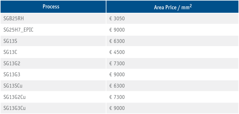
Area is one of the primary concerns of the design as it is once again a question of cold calculated economics, because, when you go to get a chip manufactured you pay per \( mm^2 \) of area.
Take for example the price quoted bellow by IHP (another fab) for their own multiwafer runs. If you participate in this run you will get back a set number of chips (40 in this case) and your final chip cost will correspond to how big your chip ultimately is.
Yet, more area is not simply more expensive because of the direct manufacturing cost, there is a second more subtle factor inflating the price, and that is yield.
Ultimately broken chips have no value, actually we could argue that we should ascribe negative value to broken chips because identifying which chips are broken costs money, and selling a customer a broken chip costs even more money. So maximizing the ratio of good chips to manufactured chips is of primary importance. This ratio is called the yield.
Chips can be broken for a plethora of reasons, but for simplicity I will put them in two different buckets. Firstly it could be a design issue, in which case all your chips are equally affected. Secondly it could be a manufacturing defect that affects your chips semi-randomly.
Manufacturing defects that occur during semiconductor device fabrication can be modeled as constant defect probability per unit of area, meaning that chips with higher area have a higher probability of having a defect, and thus lower yield, leading to ultimately higher costs.
This doesn’t impact the price which I pay to the chip area per-se, but it affects the average net price that I will pay per functional chip.
This is the double reason why area optimization is such a concern when designing chips.
Now GlobaFoundaries 180nm (gf180) is not a young node, and the polite way of calling something old is “matrue”. With node maturity comes increased expertise of the process by the foundry leading to better yields over time. So gf180 is a node with excellent yields for which area related defects are not a concern especially compared to younger leading edge nodes.
Wafer.space now offers 4 chip sizes, commonly referred to in the community as the “full”, “half”s and “quarter” slots.
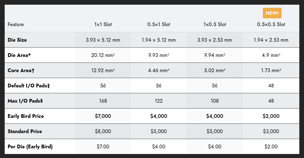
For people in need of some perspective, the full slot and its nearly 13mm2 of area is the same size as the entire Tiny Tapeout gf180 shuttle chip. The same chip that is capable of accommodating unto 160 project tiles and all the Tiny Tapeout common infrastructure. For reference, my two systolic arrays (8 bit integer and bfloat16) and the original switch all fit on only 4 tiles and my largest design to date, the blake2s hashing accelerator on 8.
Dicing#
But getting the silicon manufactured is only the first battle of the war.
Once you get your chip onto a wafer, there are two more important steps to clear before it can actually be called a chip.
Semiconductors are manufactured on a substrate called a wafer, this is a solid silicon disk that then needs to be very precisely broken up into individual chips. This step is called dicing.
So once the wafers have exited the fab and the guys at wafer.space take delivery of the full set of wafers, they call to another specialized service to dice them into individual chips along the scrible lines using a very precise diamond saw.
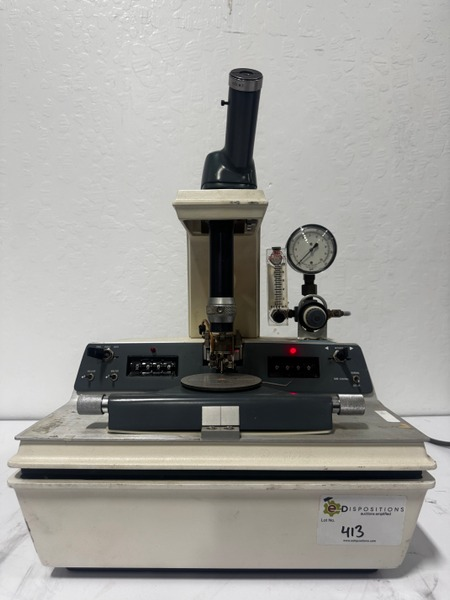
At that point, wafer.space offers two possibilities. The first is to mail you the diced chips directly, the second is to get the chips packaged for you.
Packaging ?#
Raw semiconductor silicon is beautiful but unless you are also in the habit of collecting expensive crystals to look at, they are not much use as is. After all, how do you communicate with a piece of doped silicon crystal?
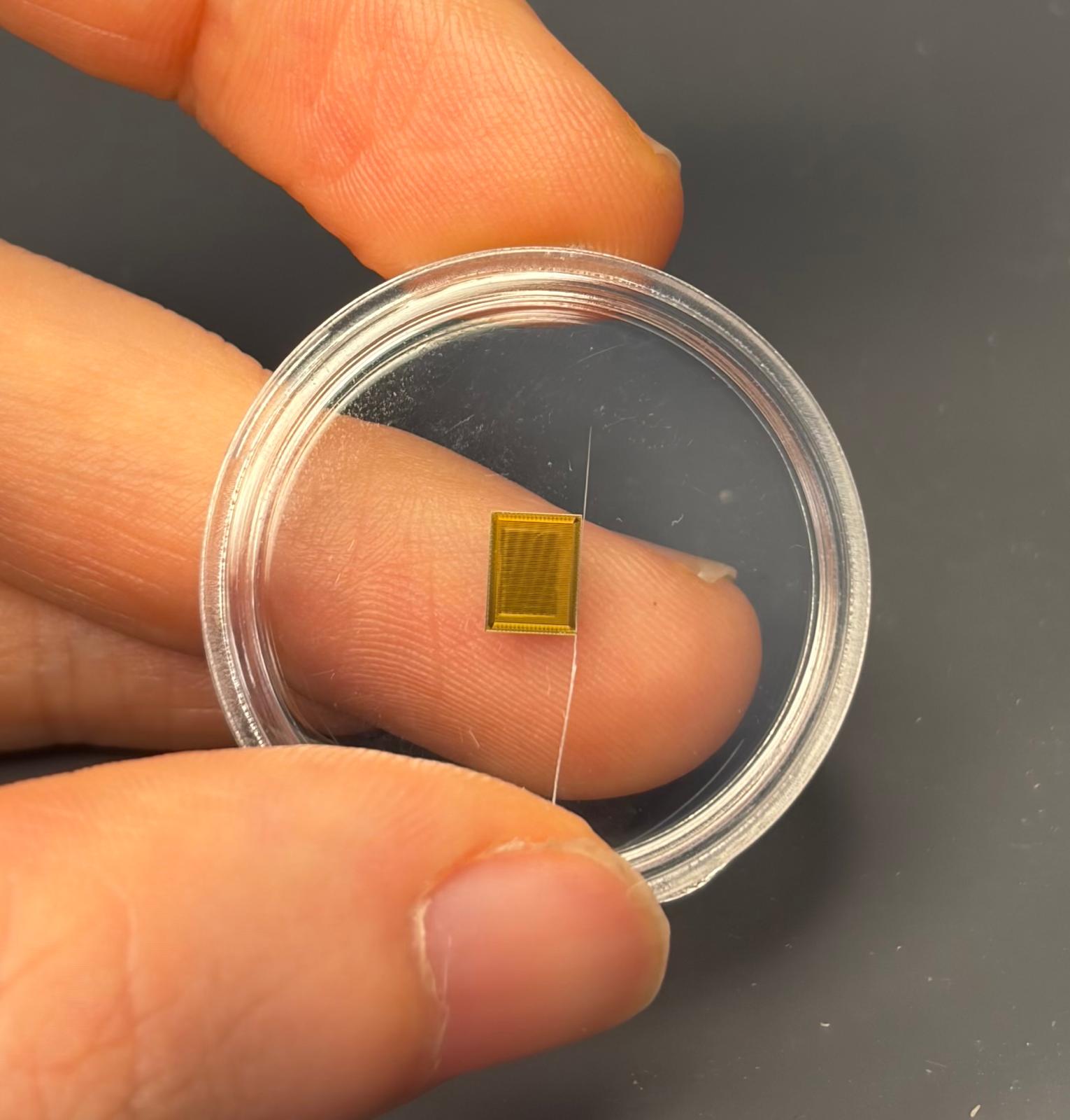
In order to both power our chip and be able to communicate with it, we need to package it in the form in which we can connect it to a wider electronic circuit.
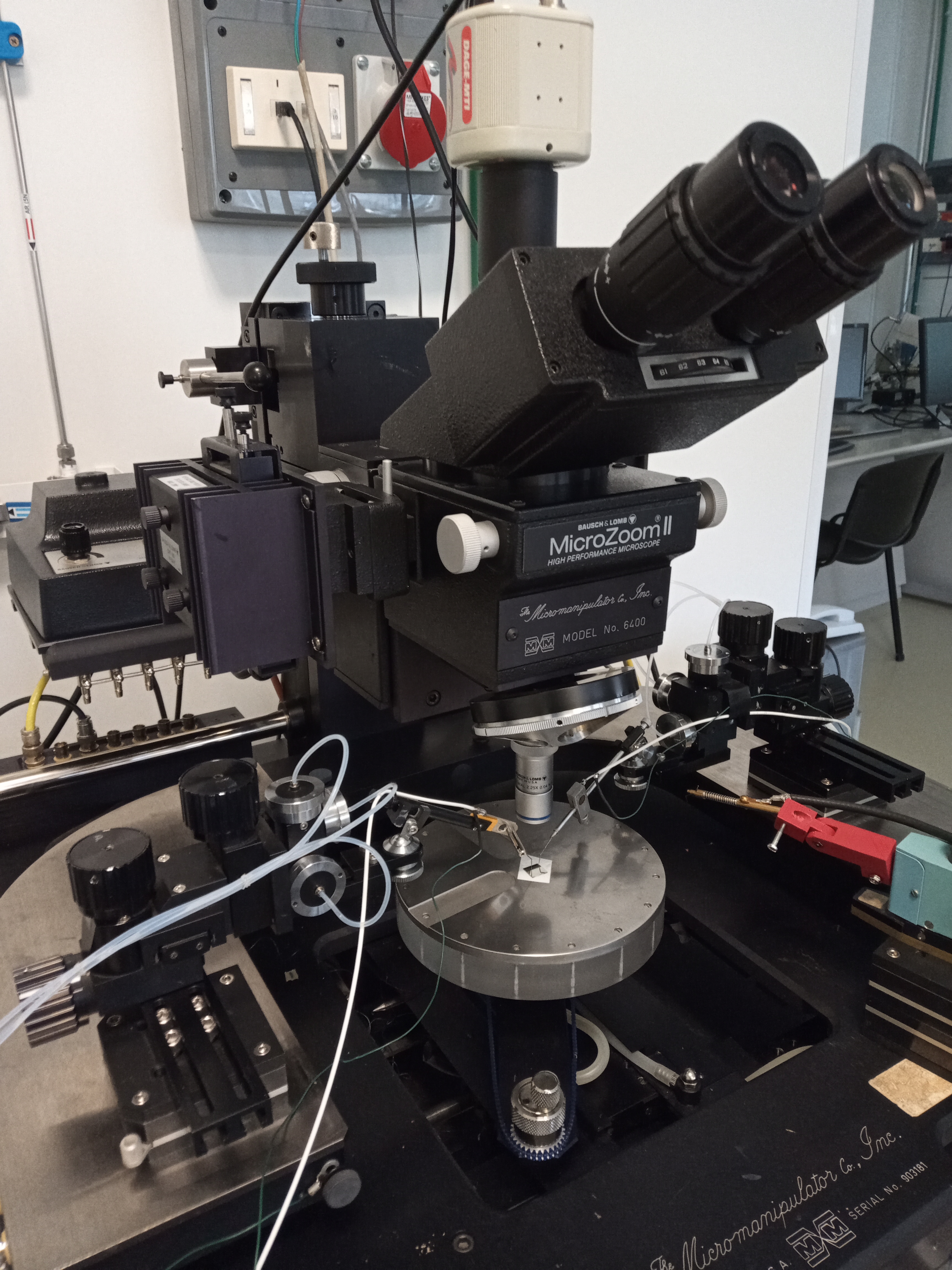
That is, unless you just happen to have a micromanipulator and about 56 microprobes lying in your garage that you can use for chip bringup. In which case please do tell me if you ever need some help clearing out your garage, I have nothing planned that day.
Chip packages come in different forms, the most common being some kind of black plastic enclosures used not only to create accessible connections to the silicon but also for protecting the delicate die and the connections from the environmental damage caused by shocks, humidity and extreme temperature fluctuations.
The type of package we chose also affects how we architect the IO and thus what our silicon floorplan will look like. There are two big families of packages:
- wire bonded
- flip-chip
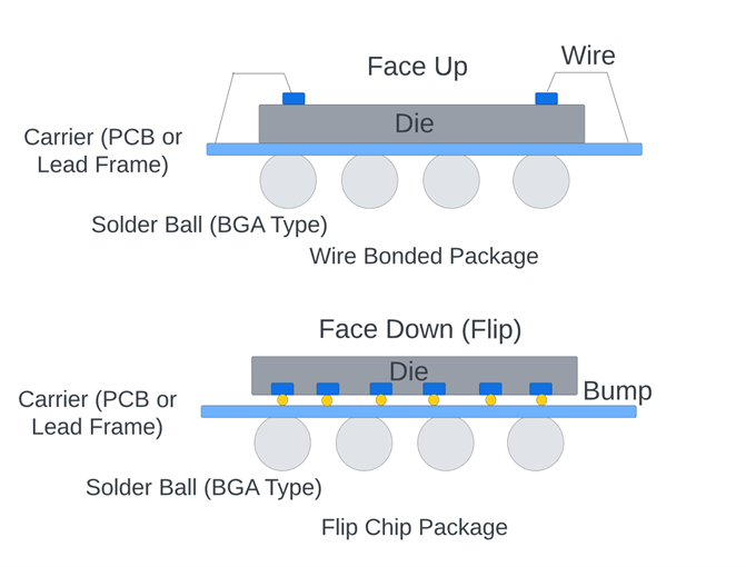
In the case of flip-chips the IO pin connections will be spread out regularly all over the floorplan leading to shorter logic to pin connections, and supporting a greater pin density and count. But on the flip side (put intended), flip chips packaging requires a lot more precision and is more expensive compared to …
Wire bonding works by conning your silicon to a pad in the package using a very thin fly wire made from gold or aluminium.
This is done by a wire bonding machine that will physically pull a wire from a IO landing pad on the silicon and connect it to a landing pad on the package. The silicon would be placed at the center of the package and would be connected to the pads placed all around it on the package, themselves connected to the larger exterior pads.
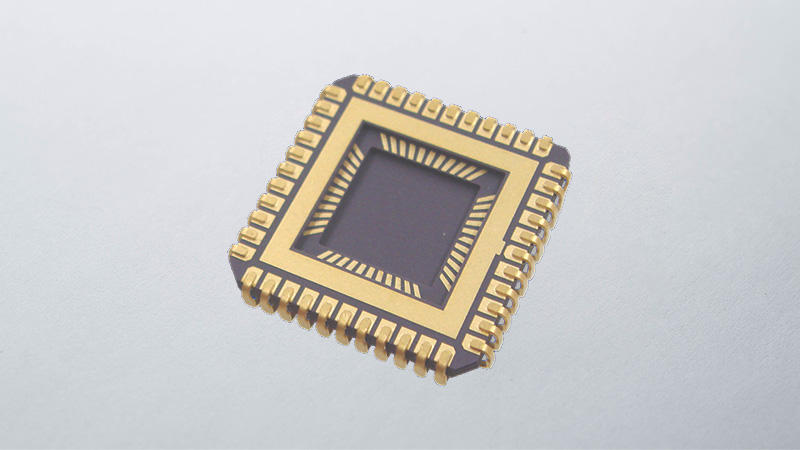
In this case the IO pad structures of the silicon would be located towards the exterior of the chip creating two distinct zones, the padring and the core region where most of the logic is located.
There are many sub-flavors of wire bonded packaging, and wafer.space decided to offer something called chip-on-board packaging (CoB), which is a bit different to how mass market chips are classically packaged but also much more cost effective for small scale fabrication.
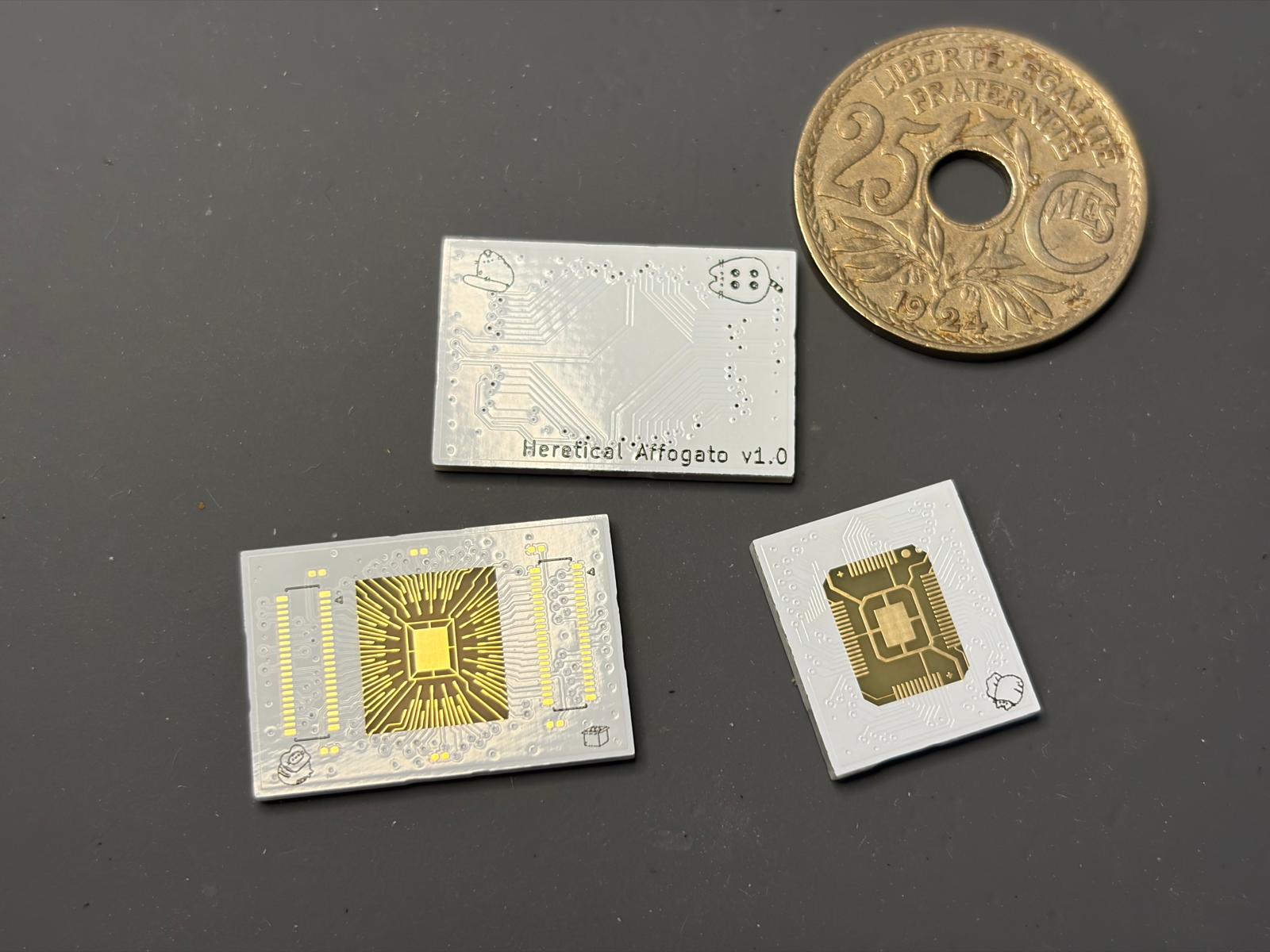
For CoB the chip is not bonded out to an enclosed package, but rather, the connections are made directly to a PCB.
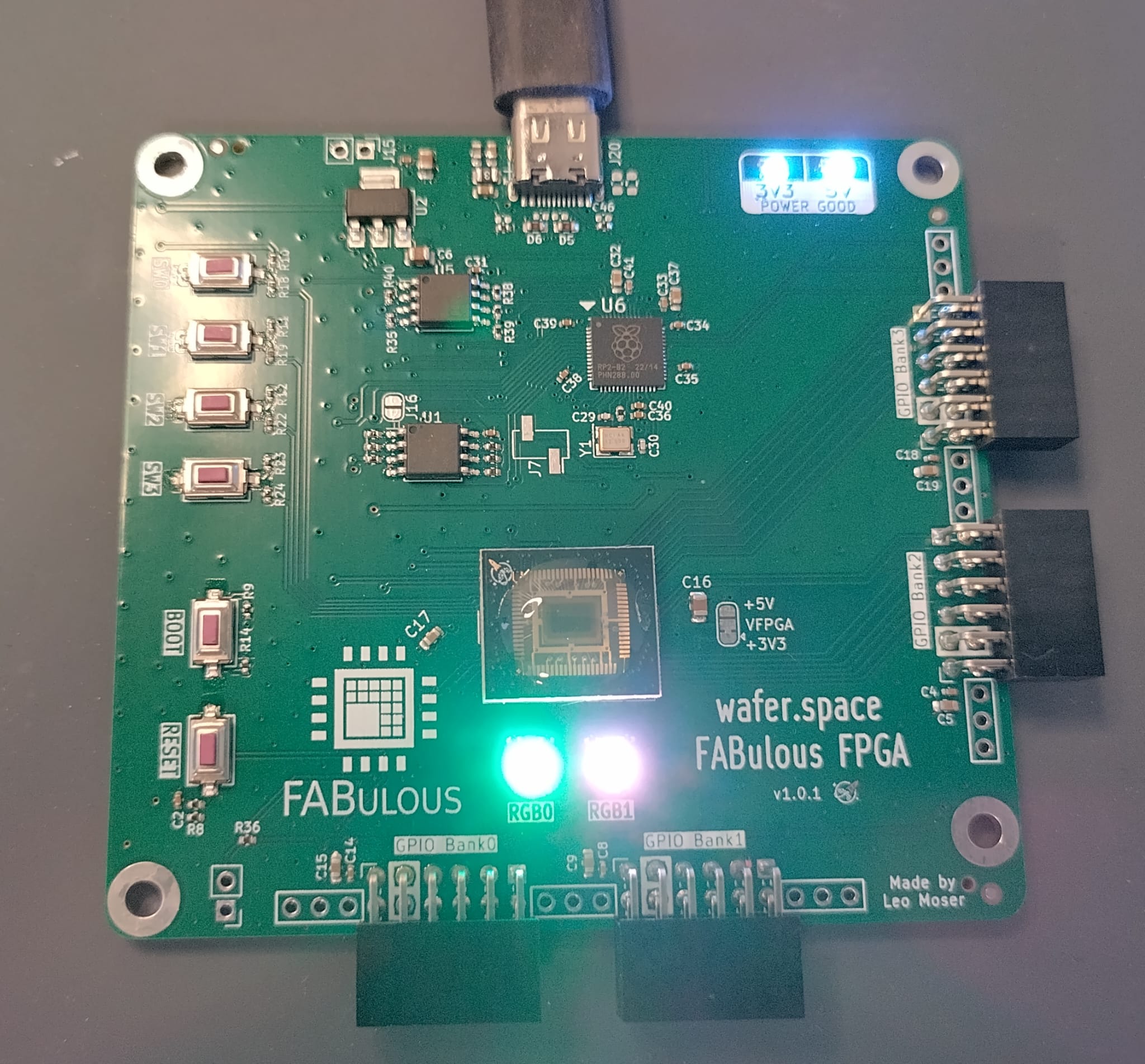
Once the chip has been bonded onto the PCB, a protective epoxy layer called a globtop is deposited and hardened on top of the silicon and the bonds. Some of you might have already noticed black blobs on commercial PCBs in the past, and without even realizing it you might have been looking at a CoB packaging.
But unlike the dull black glob tops, wafer.space has opted for the rarer beautifully transparent epoxy, allowing you to directly see the chip bonded though the package.
Take my money !#
With your silicon bonded you now have what can officially be called a chip! 🥳
What wafer.space is selling : the possibility for anyone to make their own full prototype chip run for the price of an expensive vacation, is honestly revolutionary.
DARPA and google gave us the tools, Tiny Tapeout offered us a chance to sharpen our skills and wafer.space gave us direct access to manufacturing.
Once more, in the spirit of transparency, I was invited onto the shuttle for free, but this sentiment comes from a genuine belief, so much so that as soon as the following manufacturing run sales opened I put my money where my mouth is, and bought my slot outright.

Somehow this is still cheaper than flying back for Christmas.
Chip architecture#
If you are new here and this is your first time reading this blog, welcome.
For those for whom this isn’t our first rodeo: you might be wondering how full chips differ from what I have been doing so far ?
In previous episodes, I had been taping out my designs through Tiny Tapeout. Tiny Tapeout is a shuttle chip where multiple projects share the same chip, and in doing so share a common infrastructure. That infrastructure includes handling the silicon’s IO, the power and clock distribution as well as manufacturing and sticking the chip onto a functional development boards.
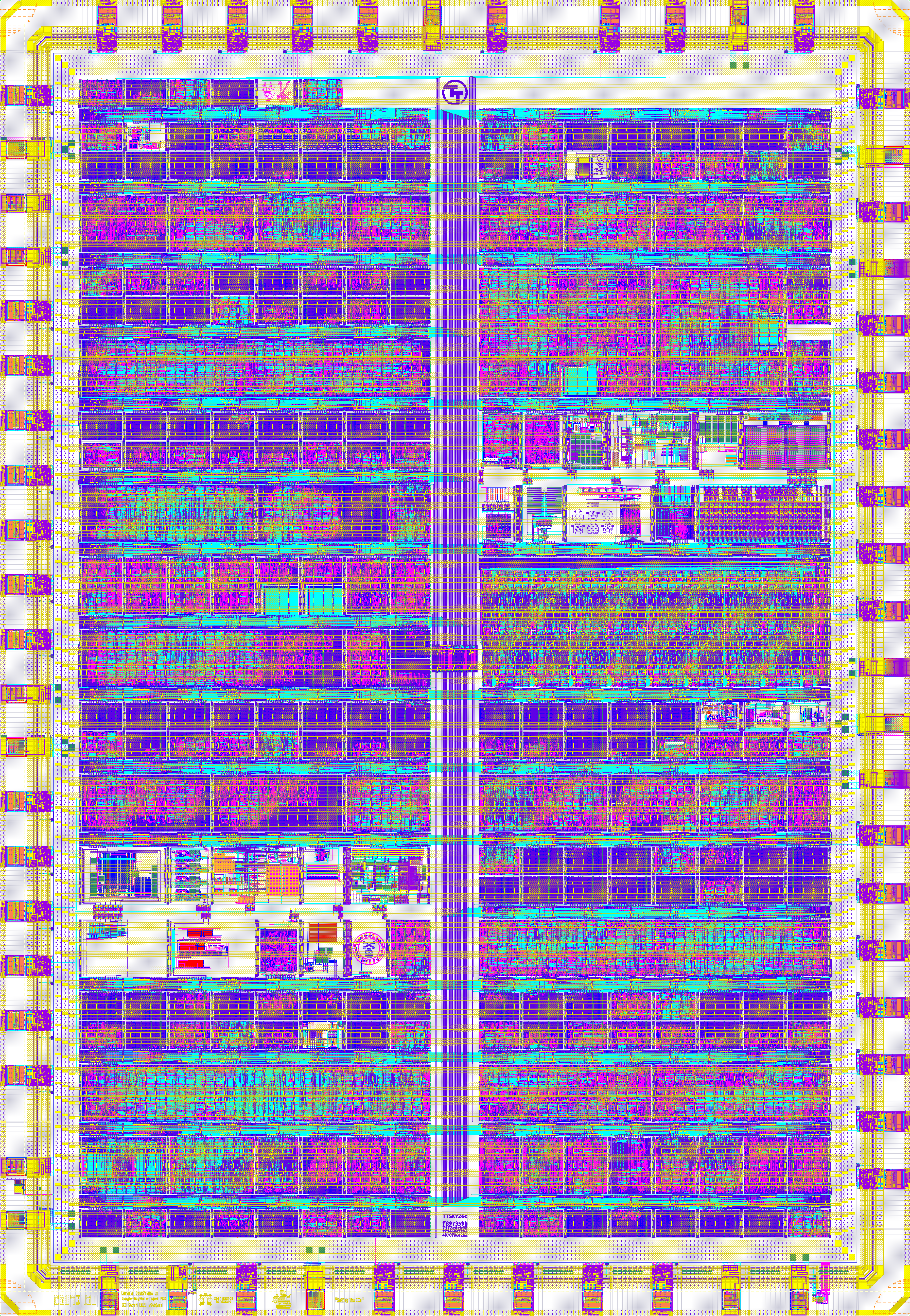
All important parts that I now get the luxury of handling on my own, which also means I also get the luxury of making all the mistakes!
But, after having gotten the chance to perfect my understanding and experience of the tapeout process through 9 prior Tiny Tapeout tapeouts this sounds the natural next step.
With Tiny Tapeout, you don’t control the number of pins, nor do you have a precise idea of the timing of the signals arriving from the chip’s pins to the pins of your macro. Additionally, even though you can buy extra tiles on Tiny Tapeout, the smallest quarter slot chip on wafer.space still gives you more core area than the largest configuration of Tiny Tapeout has to offer. And finally, Tiny Tapeout only gives you one chip per dev board, whereas with wafer.space you get a minimum order lot size of 1000 chips.
Pins#
For the purposes of the networking chip project, the real game changer is having control over the pin architecture, meaning I can now decide both the number and the type of the pins.
Because I am comunicating with the PHY chip using an RMII interface, I care very much about pins as each Ethernet port interface requires 7 pins. This was also the reason why the initial version of the networking switch had only 3 ports: I only had 24 pins.
You can refer to the previous article Designing an Ethernet Switch ASIC for an explanation on why each port needs 7 pins and each pin is used for.
So now that I have a whopping 46 pins maximum to play with, we can get cooking!
Anatomically pins are analog blocks with a landing pad for the wire bonded wire on one end. These are included as part of the GlobalFoundries open source foundry provided IO cell library, and although all the pins share the same height, width and landing pad sizes, each features different analog layouts according to its functionality.
The most important types of pins for this design are the input pins, the bidirectional pins and the power delivery pins. Have fun playing spot the difference.
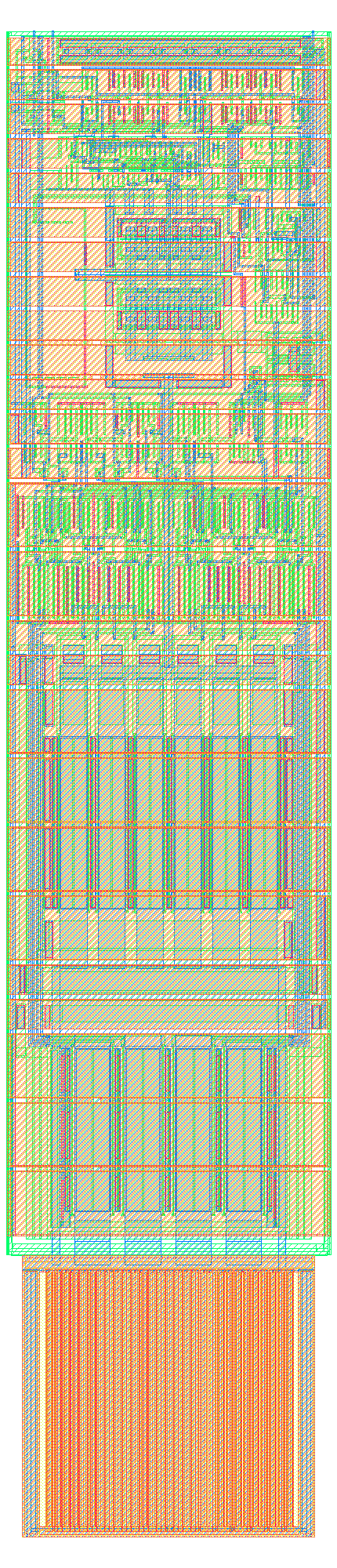
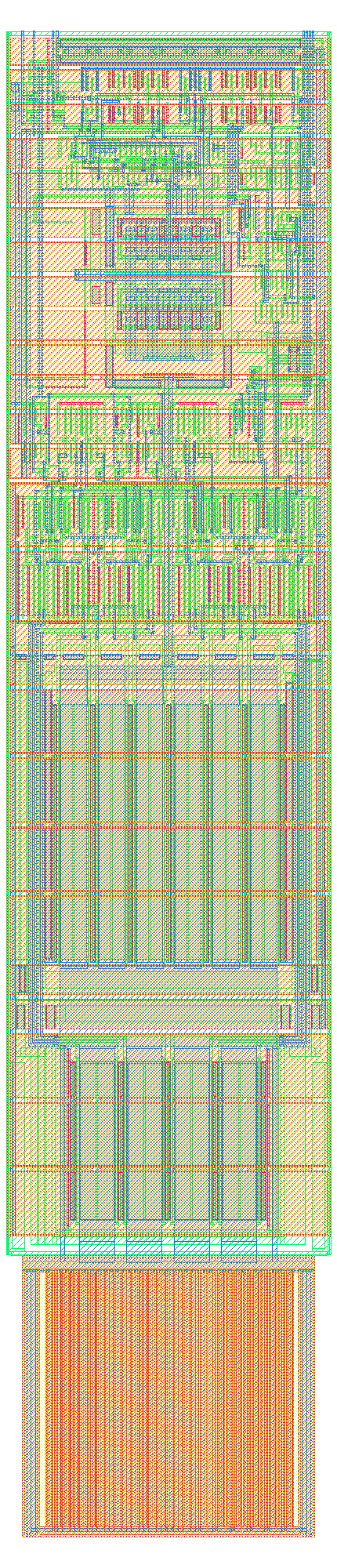
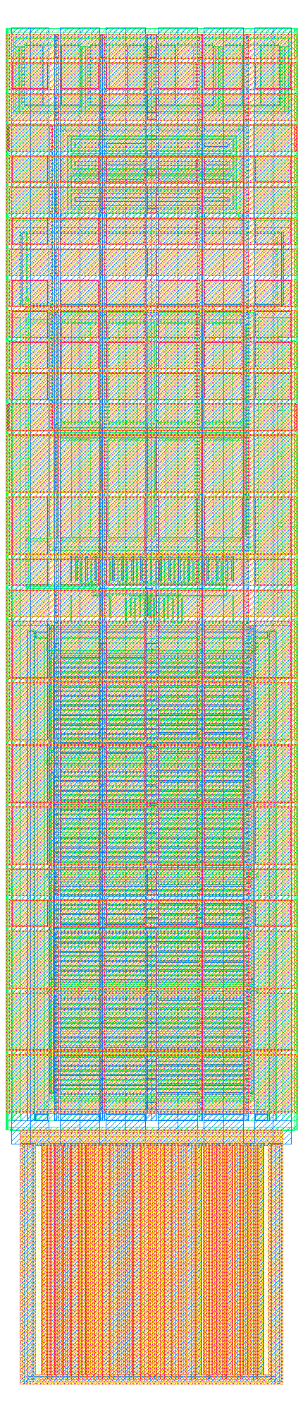
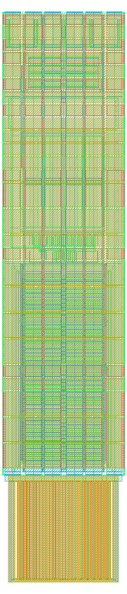
Interestingly, the standard library does not offer any pure output pins, so outputs are handled by bidirectional pins statically configured in output mode.
Looking at the floorplans provided above you might notice that these pins have no analog components directly under the landing pad, known as a “circuit under pad” design, making them a little less compact but more structurally resilient.
This is because these pins were originally designed to be compatible with a version of the GlobalFoundary 180nm process with only 3 metalization layers, but multiple levels of a metal structure must be present between the top metal layer where the pad is and the analog circuit beneath in order to help isolate it from the force applied to the pad of wedge bonding. During wedge bonding the bond is physically pressed in place requiring applying a lot of force to the silicon and potentially leading to breakages in the circuits underneath if sufficient structural support pillars aren’t present.
Padring#
As discussed earlier, there are different families of packaging for chips resulting in different types of I/O design: flip-chips and wire bonding. Wire bonded chips such as mine have their pins facing the exterior of the chip organized in a structure called a pad ring. This is a ring surrounding the core area of the chip, connecting all the different I/O pads together. This ring is used both for noise isolation and to share power between all the different pins. Because the padring is an uninterrupted crown of pins the space between the pins is filled by very simple structures called filler cells used to close the power connections within the ring.
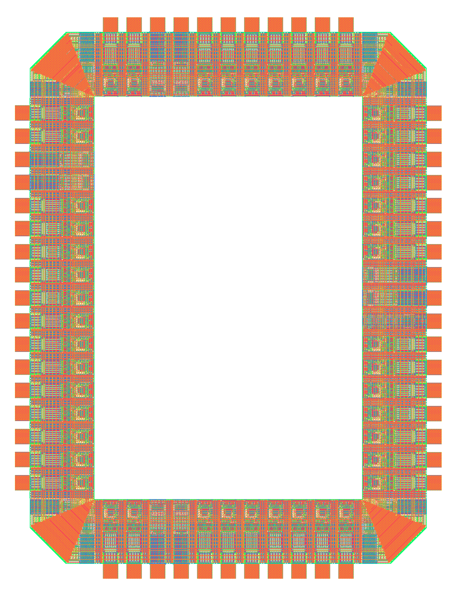
The IO also plays a crucial role in dealing with electrostatic discharge. (To whom many electronics have perished, including my little sister’s laptop that I may or may not have murdered while upgrading her ram when I was 15. 🪦 )
Each pin contains structures that will act as forward biased diodes in the event of an electrostatic discharge steering the charge though the power rails and protecting the sensitive core logic.
Power delivery#
So we actually have four types of power delivery pins : two for ground and two for power.
The difference between the two groups is that one is used to provide power to the IO itself and the other is used to power the chip’s core logic.
Thus, it is possible to run the I/O and the internal design at different voltages. The areas for which a different power source is used is called a power domain. For example, the I/O could run at 5V, accepting 5V input signals and driving 5V outputs while internally the chip core runs the logic at 3.3V. In this case, we would have different pins for powering the I/O and for powering the internal core. But, in the case of this networking chip, core power is shorted to IO power and both are in the same power domains.
Such a setup is only made possible because the foundry provided 7 track standard cell library is, to put it mildly: rugged. The cell target operating range is between 1.62 and 5.5V voltage and -40 to 125C.
So shorting the IO and core voltage and deciding to run the entire thing at 5V is just an average Tuesday.
┏━━━━━━━━━━━━━━━━━━━━━━┳━━━━━━━━━━┳━━━━━━━━━━┳━━━━━━━━━━┳━━━━━━━━━━┳━━━━━━━━━━┳━━━━━━━━━━━┳━━━━━━━━━━┳━━━━━━━━━━━┳━━━━━━━━━━┳━━━━━━━━━━━┳━━━━━━━━━━┳━━━━━━━━━━━┓
┃                      ┃ Hold     ┃ Reg to   ┃          ┃          ┃ of which ┃ Setup     ┃ Reg to   ┃           ┃ Setup    ┃ of which  ┃          ┃           ┃
┃                      ┃ Worst    ┃ Reg      ┃          ┃ Hold Vio ┃ reg to   ┃ Worst     ┃ Reg      ┃           ┃ Vio      ┃ reg to    ┃ Max Cap  ┃ Max Slew  ┃
┃ Corner/Group         ┃ Slack    ┃ Paths    ┃ Hold TNS ┃ Count    ┃ reg      ┃ Slack     ┃ Paths    ┃ Setup TNS ┃ Count    ┃ reg       ┃ Violati… ┃ Violatio… ┃
┡━━━━━━━━━━━━━━━━━━━━━━╇━━━━━━━━━━╇━━━━━━━━━━╇━━━━━━━━━━╇━━━━━━━━━━╇━━━━━━━━━━╇━━━━━━━━━━━╇━━━━━━━━━━╇━━━━━━━━━━━╇━━━━━━━━━━╇━━━━━━━━━━━╇━━━━━━━━━━╇━━━━━━━━━━━┩
│ Overall              │ 0.1951   │ 0.2897   │ 0.0000   │ 0        │ 0        │ -5.5684   │ -5.5684  │ -1272.41… │ 1065     │ 1060      │ 145      │ 2601      │
│ nom_tt_025C_3v30     │ 1.0471   │ 1.0471   │ 0.0000   │ 0        │ 0        │ 3.7457    │ 7.6040   │ 0.0000    │ 0        │ 0         │ 136      │ 1204      │
│ nom_ss_125C_3v00     │ 2.3477   │ 2.3477   │ 0.0000   │ 0        │ 0        │ -4.5534   │ -4.5534  │ -973.8862 │ 353      │ 352       │ 137      │ 2410      │
│ nom_ff_n40C_3v60     │ 0.4488   │ 0.4878   │ 0.0000   │ 0        │ 0        │ 4.6815    │ 12.7768  │ 0.0000    │ 0        │ 0         │ 136      │ 532       │
│ min_tt_025C_3v30     │ 1.0388   │ 1.0388   │ 0.0000   │ 0        │ 0        │ 3.7448    │ 8.0005   │ 0.0000    │ 0        │ 0         │ 130      │ 1149      │
│ min_ss_125C_3v00     │ 2.3336   │ 2.3336   │ 0.0000   │ 0        │ 0        │ -3.7267   │ -3.7267  │ -764.3782 │ 296      │ 295       │ 131      │ 2304      │
│ min_ff_n40C_3v60     │ 0.4466   │ 0.4826   │ 0.0000   │ 0        │ 0        │ 4.6844    │ 12.9664  │ 0.0000    │ 0        │ 0         │ 130      │ 481       │
│ max_tt_025C_3v30     │ 1.0579   │ 1.0579   │ 0.0000   │ 0        │ 0        │ 3.7465    │ 7.0758   │ 0.0000    │ 0        │ 0         │ 141      │ 1320      │
│ max_ss_125C_3v00     │ 2.3651   │ 2.3651   │ 0.0000   │ 0        │ 0        │ -5.5684   │ -5.5684  │ -1272.41… │ 416      │ 413       │ 142      │ 2601      │
│ max_ff_n40C_3v60     │ 0.4527   │ 0.4945   │ 0.0000   │ 0        │ 0        │ 4.6771    │ 12.4714  │ 0.0000    │ 0        │ 0         │ 140      │ 641       │
│ nom_tt_025C_5v00     │ 0.5200   │ 0.6317   │ 0.0000   │ 0        │ 0        │ 4.5785    │ 11.4278  │ 0.0000    │ 0        │ 0         │ 139      │ 673       │
│ nom_ss_125C_4v50     │ 1.1099   │ 1.3887   │ 0.0000   │ 0        │ 0        │ 3.5360    │ 4.4721   │ 0.0000    │ 0        │ 0         │ 139      │ 1444      │
│ nom_ff_n40C_5v50     │ 0.1981   │ 0.2942   │ 0.0000   │ 0        │ 0        │ 5.0271    │ 14.5140  │ 0.0000    │ 0        │ 0         │ 139      │ 249       │
│ min_tt_025C_5v00     │ 0.5113   │ 0.6248   │ 0.0000   │ 0        │ 0        │ 4.5846    │ 11.6500  │ 0.0000    │ 0        │ 0         │ 133      │ 648       │
│ min_ss_125C_4v50     │ 1.0892   │ 1.3768   │ 0.0000   │ 0        │ 0        │ 3.5474    │ 4.8628   │ 0.0000    │ 0        │ 0         │ 134      │ 1365      │
│ min_ff_n40C_5v50     │ 0.1951   │ 0.2897   │ 0.0000   │ 0        │ 0        │ 5.0285    │ 14.6577  │ 0.0000    │ 0        │ 0         │ 132      │ 223       │
│ max_tt_025C_5v00     │ 0.5316   │ 0.6407   │ 0.0000   │ 0        │ 0        │ 4.5719    │ 11.1135  │ 0.0000    │ 0        │ 0         │ 143      │ 784       │
│ max_ss_125C_4v50     │ 1.1382   │ 1.4034   │ 0.0000   │ 0        │ 0        │ 3.5178    │ 3.8667   │ 0.0000    │ 0        │ 0         │ 145      │ 1518      │
│ max_ff_n40C_5v50     │ 0.2026   │ 0.3003   │ 0.0000   │ 0        │ 0        │ 5.0257    │ 14.3356  │ 0.0000    │ 0        │ 0         │ 143      │ 449       │
└──────────────────────┴──────────┴──────────┴──────────┴──────────┴──────────┴───────────┴──────────┴───────────┴──────────┴───────────┴──────────┴───────────┘
Example of a random timing report from another chip I am working on, with corners ranging from 3 to 5.5V and -40 to 125C. And again, this is still just a subset of all the corners there are: there are even more where this came from!
For reference, this is just a tiny bit unusual.
Most designs have separate power domains as modern nodes have cell libraries designed for much lower operating voltages in order to help reduce the area power density making cooling easier and to help optimize power consumption. In the case of leading edge nodes, internal logic targets operating voltages as low as 0.7 to 0.8 V. This forces having at least separate IO and core power domains, since your IO typically starts at 1.8V and above.
Yet, you sometimes need separate power domains even if they operate at the same voltage, such as cases where you want to isolate a sensitive analog block from the power supply noise caused by a quickly toggling digital part. You might even prolong this separation of an analog and digital power domains to the IO, in which case rather than having a fully connected padring working within the same power domain you would be splitting the padding into analog IO power and digital IO power.
Remember the filler cells I talked about earlier? Well there exists a special type of filler cell called a splitter used specially to split the pad ring in such cases. But, because of ESD concerns this splitter is not as simple as breaking the power line, but that is a discussion for another day.
Clock and reset#
The clock for this chip is supplied though a Schmitt trigger input pin and is strategically logged in the corner of the chip right next to the reset signal, and isolated from the rest of the pins by two power pins. This is done to limit the clock signal’s impact onto the neighboring pins given its toggle frequency, as well as to prevent the clock signal for the neighboring pins cross talk. The reset signal by comparison is a very stable signal producing little crosstalk of its own.
From this point on the clock signal is pulled into the center of the floorplan and then distributed through a balanced clock tree throughout the chip.
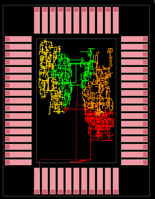
Such “shielding” is even more important in our case since we are doing wire bonding and we can also have cross talk between signals occurring between the fly wires, this would be less of a problem for a flip-chip package.
Zhe switch#
This is a different challenge compared to what I was doing with Tiny Tapeout as I now have access to two great resources: firstly, a lot more pins to play with, and secondly, a lot more space. Even if I target the smallest possible chip, I am still blessed with more area than I know what to do with.
Even before being invited to contribute I was already eyeing the wafer.space slots, so selecting the switch at the crown project of the ASIC was the easy choice.
The problem is that the switch was initially designed for the constraints of Tiny Tapeout. As such, not only does it have an odd architecture with only three ports, but it was designed to be as space efficient as possible. Here, space is something I am swimming in, but with only 96 hours ahead of me I have no time to redesign an entirely new switch from scratch. So the plan is to re-adapt the existing switch to make the best use of being its own chip.
The first and the most important change was to be able to make use of these abundant pins and have the switch to support more ports.
No longer shall I be constrained by my pin count! 🔥 w 🔥
… (Until I need more than 7 ports that is.)
Parameters#
Most of the verilog code you will see online tends to use hard coded widths like so :
module add(
	input wire [7:0] a_i,
	input wire [7:0] b_i,
	output wire [7:0] res_o,
	output wire carry_o
);
	assign {carry_o, res_o} = a_i + b_i;
endmodule
What this code gains in ease of writing it loses in flexibility.
In RTL, we have a concept called parameters, which exist for an instance of a module and allow you to define, at instantiation, certain values. These values can then be used to size up buses or are macro like conditions to define which sections of the code should be included in the final hardware.
module add#(
	parameter W = 8
)(
	input wire [W-1:0] a_i,
	input wire [W-1:0] b_i,
	output wire [W-1:0] res_o,
	output wire carry_o
);
	assign {carry_o, res_o} = a_i + b_i;
endmodule
These generic values can then be inherited down the design hierarchy allowing dependent modules to be resized accordingly.
Complexity#
The original switch implementation was partially generic : it contained quite a few generic values, but these were mostly added out of habit to help clean up the design and keep things more readable, rather than truly making the design dimensions fully configurable.
The reason for not making the design fully generic was out of a calculated decision to shy away from as much unnecessary complexity as possible. The original design was facing the hard physical constraints of Tiny Tapeout pin count, so making it fully generic to support an arbitrary amount of ports would have been an unnecessary premature optimization, and most importantly cost complexity.
My grief against complexity comes from two calculated trade-offs.
First, I find it is orders of magnitude cheaper to add complexity than to remove it.
Secondly, complexity is especially expensive for hardware design because of the necessity to not have no have any bugs in the hardware. The only way of reaching this bug free state is through thought verification of operation under all possible scenarios. As we add complexity, we add hardware states such that the size of the space of states we need to explore grows exponentially.
Now I know exponential growth might sound like an exaggeration, after all exponential growth is so fast that it is hard for our brains to conceive, but I assure you I am not.
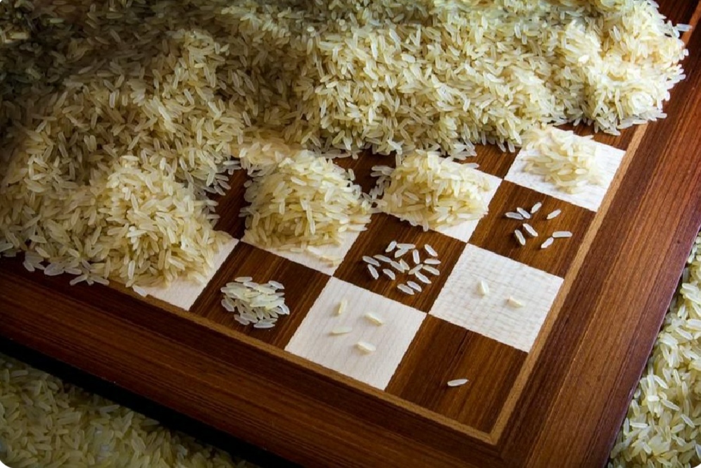
This problem is more formally called the “state explosion problem”.
Scale Up#
So the biggest change in the switch was to move the number of supported ports from a static three to a generic number.
Even if the RTL scales, and I could theoretically run a simulation with 48 ports, the logic itself still has scaling limits. After all, behind the abstraction of the code we are designing hardware logic for which physical constraints still apply.
As the structures get wider, the number of logic elements on a path increases, the paths get physically longer and the timing degrades. And so, with \(1.73mm^2\) of core area available, timing is the wall I hit first.
Given the switch was already quite tight on timing, scaling it too far would push it beyond the limits of the current design requiring a rethink of the architecture. Rethink that I cannot afford to execute in so little time.
Lastly, I said I was scaling the number of ports, but because of how tight the timings are on the switch lookup table already was, it is not getting scaled up. And because it still only has four entries, and scaling beyond four ports would result in too much contention on the table and not enough hits, it would not make any sense to go beyond 4 ports for now.
Thus, I settled on four ports for the switch.
Pin correspondance#
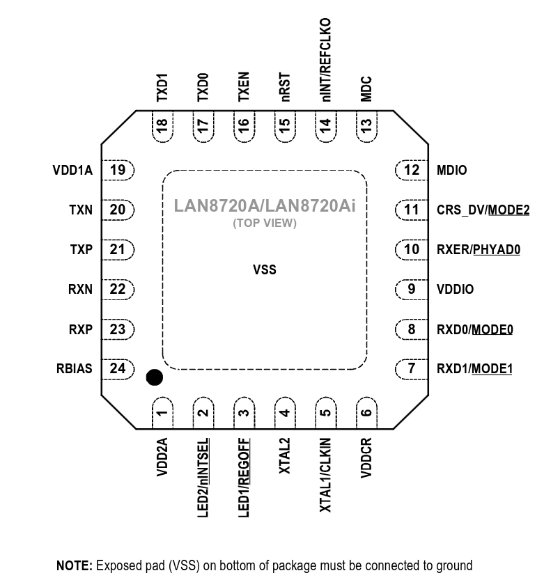
Given I now control the full ASICs layout I can also control exactly which signal maps to which pin on the padring.
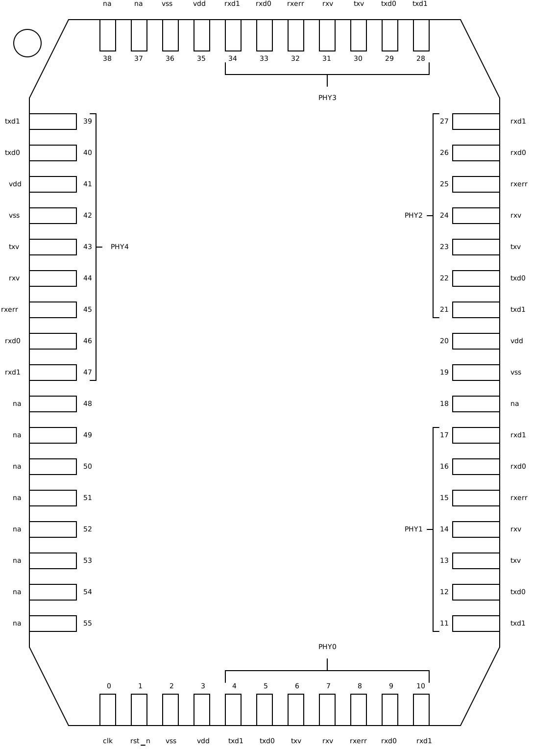
Since the switch was intended to work with a specific Microchip family of external physical-layer chips, and that these chips had a known pinout, I decided to choose the pin order based on how directly I could draw the connecting wire onto the PCB.
Beacon#
One of the best drawbacks of the switch scaling limit was that I was left with a few pins and lots of area to play with.
And unlike with Tiny Tapeout where multiple projects share that same common infrastructure allowing only one project to be enabled at a time, this time I could have multiple designs working in parallel. And I had just the perfect project to include in parallel.
A few months back I did the two things the entire Internet knows not to do: firstly I asked Reddit for advice, secondly I followed it.
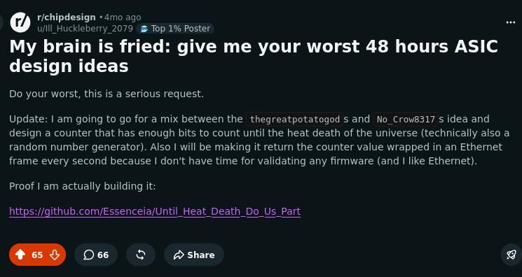
This project is called “Until Heat Death Do Us Part" and is a very serious implementation of an ethernet connected beacon that broadcasts its current time over 100 Mbit Ethernet with the ability to do so without overflow for the next \(10^{100}\) years. Also believed to be roughly the estimated heat death of the universe, give or take a few powers of 10 years.
I have a full write-up about this ASIC’s here for those interested in getting the full story: Until Heat Death Do Us Part.
Full chip#
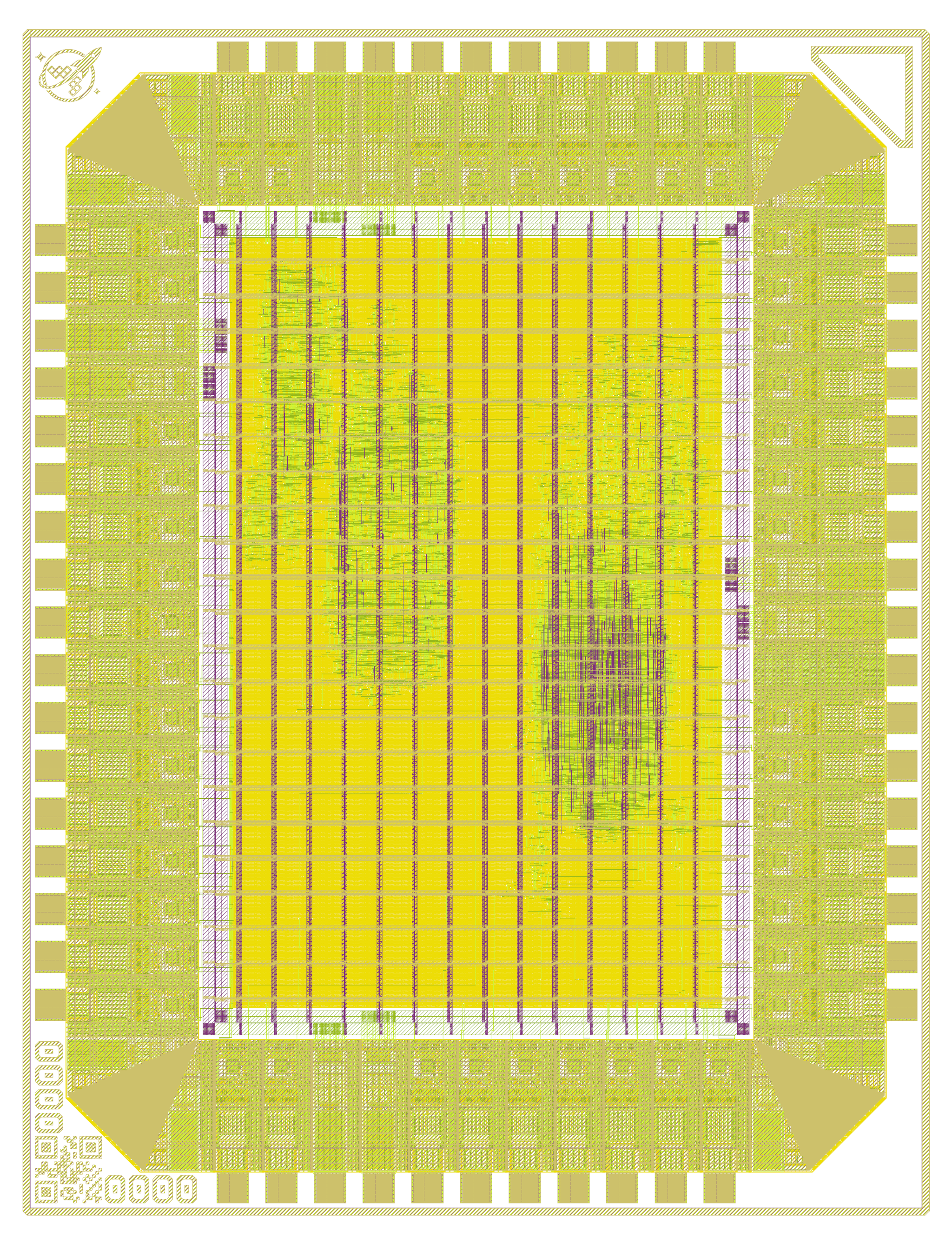
Putting it all together: this chip features two designs, the 4 port 100Mbps networking switch and the ethernet broadcast beacon. The networking switch is the denser design on the right hand side of the floorplan with the beacon being the on the left side, each designed placed next to there respective port pins.
What comes next?#
It’s already been a few months since the chip has been sent to the fab. Since then the first batch of produced wafers have exited the fab and been received by the wafer.space.
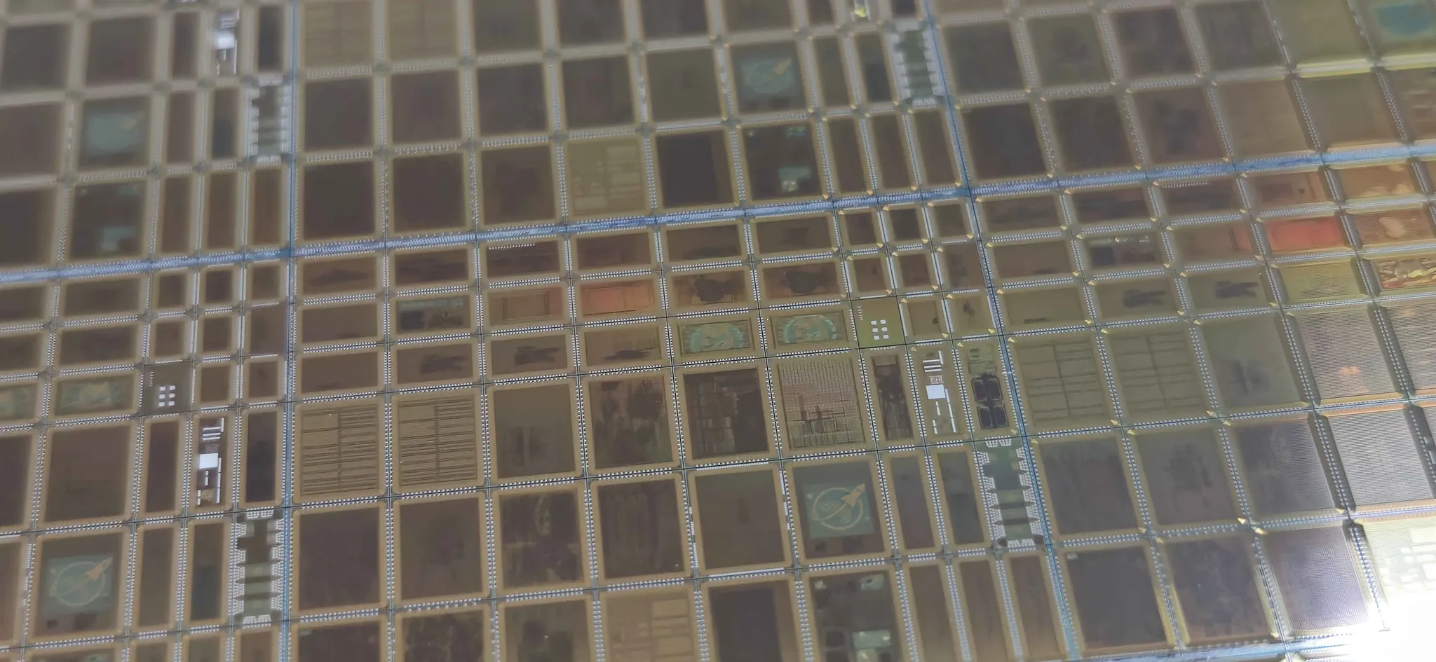
Andrew Wingate shared with us some absolutely gorgeous pictures of the diced wafers, and there is my little chip in the flesh sitting on the top right corner of the reticle:
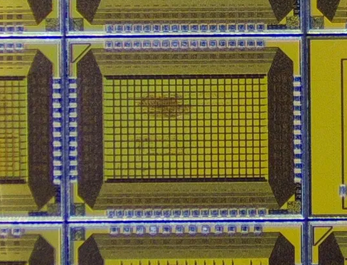
The dies are then picked off the diced wafer using a custom built robot and sorted per chip type into a tape reel. From there the chips will be either sent to the bond house for packaging or directly sent to the customer.
And now I am like a child waiting for Christmas, impaciently awaiting a package, inside the first batch of my own full custom ASIC chips.
Now, the chip doesn’t make a full networking equipment on its own, which is why I am also prototyping a PCB for the switch. Hopefully someday I can plug the chip in to get a fully functional switch.
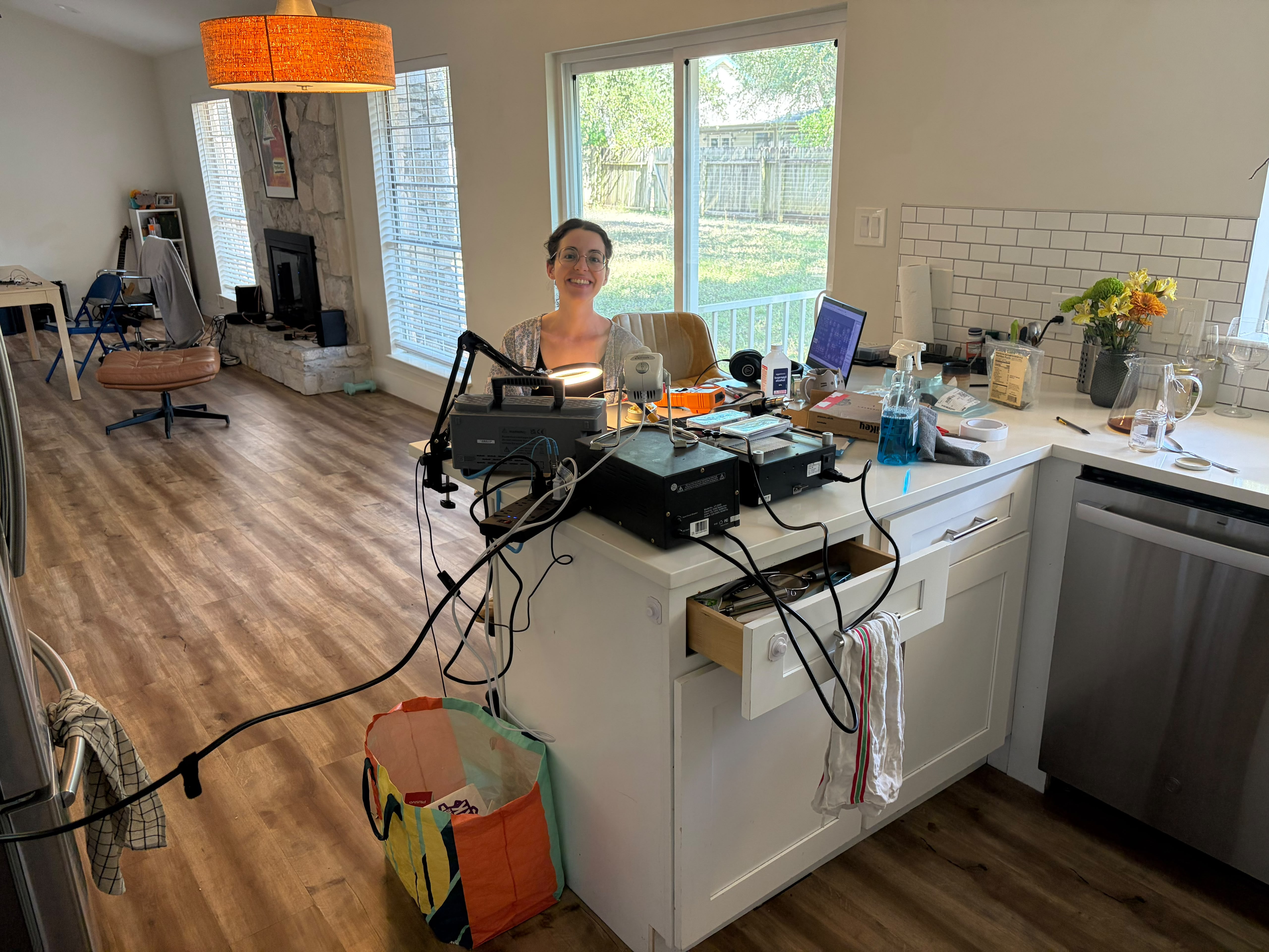
Here is to hoping the first iteration of the silicon just works !
.. which anyone working in the industry can attest to, A0s are rare enough to be legendary.
Manufacturing revisions of a chip are identified by a letter followed by a number.
A0 is the first iteration, minor revision such as changing some of the higher metalization layers will increment the number and major revisions requiring a new mask set for the bottom layers, where the transistors are built, increment the letter and reset the number. So revisions might go: A0, A1, A2, B0, B1, B2, B3, C0, etc…
Meanwhile the networking equipment project continues, chasing after building increasingly complex systems. Without going too deep into which next networking features I want to add, it is becoming quickly apparent that I will need to integrate some form of a CPU.
This is because as I target more advanced networking applications the tasks my silicon needs to accomplish become increasingly varied and start featuring a large array of tasks that occur rarely enough, and have sufficiently lax performance requirements to be better suited for software than hardware.
As for the matter of which CPU architecture to choose, although RISC-V is in vogue I find that, as a result of RISC-V’s architectural choices, it is just too expensive to implement in terms of area for systems like mine.
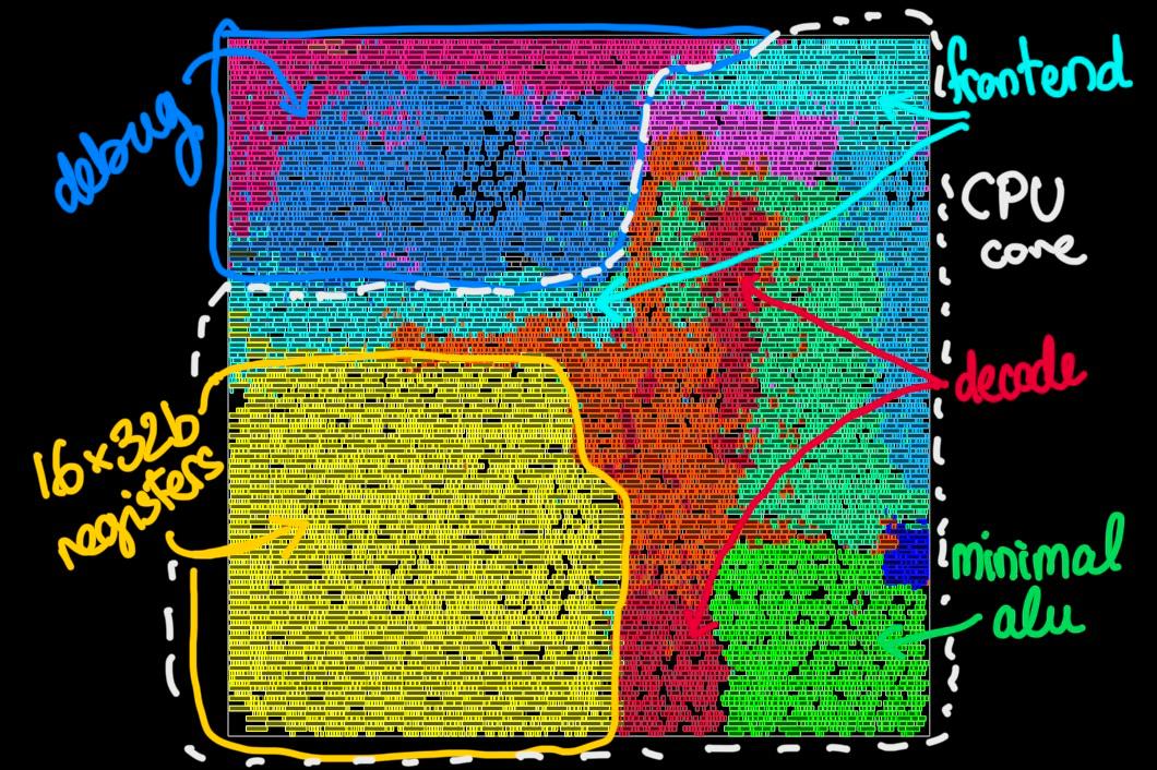
My needs when selecting witch CPU architecture to use are:
- be cheap to implement in hardware
- have a pre-existing software ecosystem, meaning having C compiler and debugger support
- not get me sued
If only gcc were to maintain something like the “Status of Supported Architectures from Maintainers’ Point of View” at https://gcc.gnu.org/backends.html then maybe I could know what my options where.
Architecture characteristic key
-----------------------------------------------------------------------
H       A hardware implementation does not exist.
M       A hardware implementation is not currently being manufactured.
S       A Free simulator does not exist.
L       Integer registers are narrower than 32 bits.
Q       Integer registers are at least 64 bits wide.
N       Memory is not byte addressable, and/or bytes are not eight bits.
F       Floating point arithmetic is not included in the instruction set
I       Architecture does not use IEEE format floating point numbers
C       Architecture does not have a single condition code register.
B       Architecture has delay slots.
D       Architecture has a stack that grows upward.

l       Port cannot use ILP32 mode integer arithmetic.
q       Port can use LP64 mode integer arithmetic.
r       Port can switch between ILP32 and LP64 at runtime.
        (Not necessarily supported by all subtargets.)
p       Port uses define_peephole (as opposed to define_peephole2).
b       Port uses '"* ..."' notation for output template code.
f       Port does not define prologue and/or epilogue RTL expanders.
m       Port does not use define_constants.
g       Port does not define TARGET_ASM_FUNCTION_(PRO|EPI)LOGUE.
i       Port generates multiple inheritance thunks using
        TARGET_ASM_OUTPUT_MI(_VCALL)_THUNK.
a       Port uses LRA (by default, i.e. unless overridden by a switch).
t       All insns either produce exactly one assembly instruction, or
        trigger a define_split.
e       <arch>-elf is not a supported target.
s       <arch>-elf is the correct target to use with the simulator
        in /cvs/src.

          |      Characteristics
Target     | HMSLQNFICBD lqrpbfmgiates
-----------+--------------------------
aarch64    |     Q        q  b  gia  s
alpha      |  ?  Q   C    q    mgi  e
arc        |          B      b  gia
arm        |                 b   ia  s
avr        |    L  FI    l  p   g a
bfin       |       F            gi
bpf        | HM  Q FIC   lq  b    a
c6x        |   S     CB         gi
cris       |       F  B         gia  s
csky       |                 b   ia
epiphany   |         C          gia  s
fr30       | ??    FI B     pb mg    s
frv        | ??       B      b   i   s
gcn        |   S     C D  q       a e
h8300      |       FI B         g a  s
i386       |     Q        q  b   ia
ia64       |   ? Q   C    qr b m i
iq2000     | ???   FICB      b  g at
lm32       |       F            g
m32c       |    L  FI    l   b  g    s
m32r       |       FI        b    a  s
m68k       |                pb   i
mcore      |  ?    FI       pb mg    s
mep        |       F C       b  g  t s
microblaze |         CB          ia  s
mips       |     Q   CB   qr     ia  s
mmix       | HM  Q   C    q      ia e
mn10300    | ??                 gi   s
moxie      |       F            g  t s
msp430     |    L  FI    l   b  g    s
nds32      |       F C           ia  s
nios2      |         C           ia
nvptx      |   S Q   C    q    mg   e
pa         |     Q   CBD  qr b   i  e
pdp11      |    L   IC    qr b      e
pru        |    L  F              a  s
riscv      |     Q   C    qr    gia
rl78       |    L  F     l      g    s
rs6000     |     Q   C    qrpb   ia
rx         |                         s
s390       |     Q        qr    gia e
sh         |     Q   CB   qrp    i
sparc      |     Q   CB   qr b   ia
stormy16   | ???L  FIC D l   b   ia
v850       |                    g a  s
vax        |  M     I        b   i  e
visium     |          B         g  t s
xtensa     |         C
Behold: so many beautiful options supported that most people have never even heard of!
And within this list there is one 16 bit architecture that caught my eye, at the heart of one of the longest produced systems and deeply intertwined with computer history as it saw the first version of Unix written in C.
What better choice than a PDP-11?
Closing#
A year ago, I started on a journey to go from being solely a hardware designer to building an entire ASIC from scratch without any institutional backing.
It’s been a long road, passing though multiple smaller macro tapeouts, each allowing me to delve deeper into what it takes to make ASICs. This chip is my 10th solo tapeout, a fitting number to finally graduate into building full chips.
Standing upon this mountain I can tell you the road ahead is still very long.
And with my first batch of full custom ASICs landing into my mailbox in a few weeks a new risk has emergeded, leading me to proclaim a new goal: not starting a fabless semiconductor company.
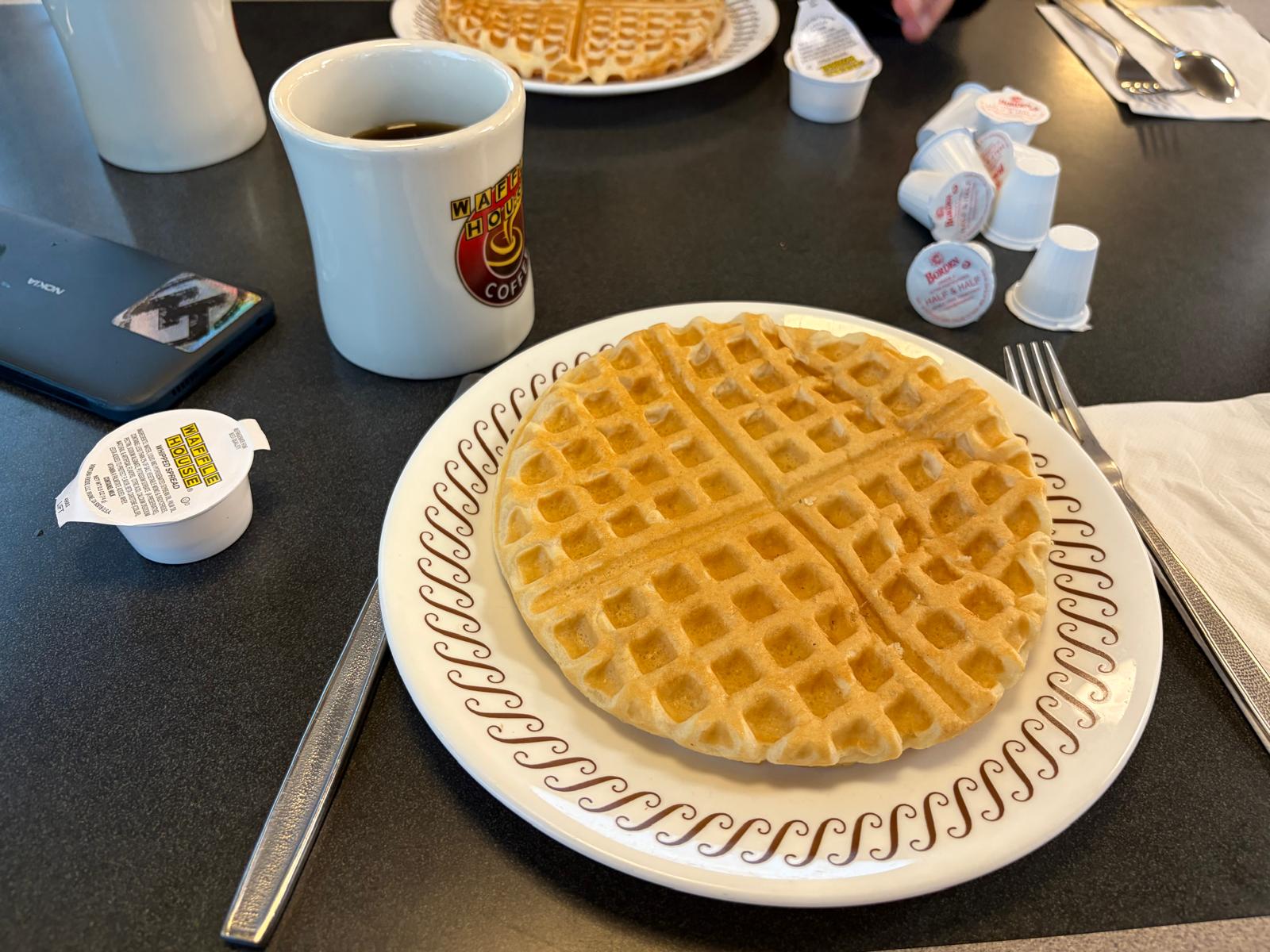
Current life goals
- Have kids
- Spend time with loved ones
- Make chips
- Eat waffles
- Get a wire bonder
- Not get a job
- Not startting a fabless semiconductor company 🆕
Thanks again to wafer.space for giving me this opportunity to join the shuttle, Tiny Tapeout for making the 9 previous tapeouts possible and the open source silicon community for building the tools making all of this possible.
If you enjoyed this, I will be sipping coffee at a Silicon Valley neighborhood cafe between the 10th and 12th of November, so if you feel like nerding out over caffeine shoot me an email.